PCM1753
PCM1754
PCM1755
www.ti.com
SLES092A – OCTOBER 2003 – REVISED AUGUST 2004
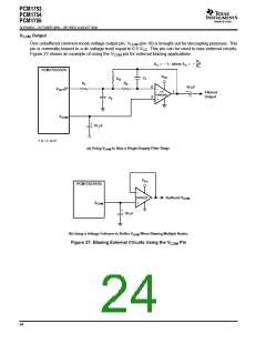
APPLICATION INFORMATION
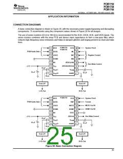
CONNECTION DIAGRAMS
A basic connection diagram is shown in Figure 28, with the necessary power supply bypassing and decoupling
components. TI recommends using the component values shown in Figure 28 for all designs.
The use of series resistors (22 Ω to 100 Ω) is recommended for the SCK, LRCK, BCK, and DATA inputs. The
series resistor combines with the stray PCB and device input capacitance to form a low-pass filter, which
reduces high-frequency noise emissions and helps to dampen glitches and ringing present on clock and data
lines.
PCM1753
PCM1755
System Clock
BCK
SCK
ML
1
2
3
4
5
6
7
8
16
15
14
13
12
11
10
9
PCM Audio Data
DATA
LRCK
DGND
NC
Register Control
MC
MD
ZEROL/NA
Zero Mute Control
V
CC
ZEROR/ZEROA
+5 V
10 mF
V
V
L
V
COM
OUT
+
10 µF
10 µF
R
AGND
OUT
10 mF
Post LPF
L-Ch Out
Post LPF
R-Ch Out
PCM1754
System Clock
BCK
SCK
FMT
1
2
3
4
5
6
7
8
16
15
14
13
12
11
10
9
PCM Audio Data
Format
DATA
LRCK
DGND
NC
MUTE On/Off
DEMP On/Off
MUTE
DEMP
TEST
Zero Mute Control
V
CC
ZEROA
+5 V
10 mF
V
V
L
V
COM
OUT
+
10 µF
10 µF
R
AGND
OUT
10 mF
Post LPF
L-Ch Out
Post LPF
R-Ch Out
Figure 28. Basic Connection Diagram
25

 BB [ BURR-BROWN CORPORATION ]