PCM1753
PCM1754
PCM1755
SLES092A – OCTOBER 2003 – REVISED AUGUST 2004
www.ti.com
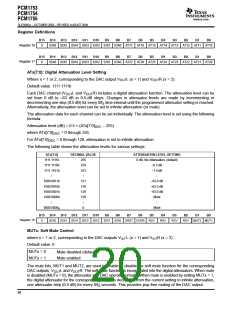
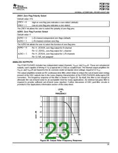
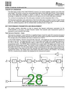
V
Output
COM
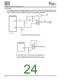
One unbuffered common-mode voltage output pin, V
(pin 10) is brought out for decoupling purposes. This
COM
pin is nominally biased to a dc voltage level equal to 0.5 V . This pin can be used to bias external circuits.
CC
Figure 27 shows an example of using the V
pin for external biasing applications.
COM
R2
R1
AV + *1, where AV + *
PCM1753/54/55
V
CC
C
1
R
2
R
1
R
3
2
3
10 µF
†
–
V X
OUT
1/2
1
Filtered
Output
OPA2353
C
2
+
V
COM
+
10 µF
†
X = L or R
(a) Using V
to Bias a Single-Supply Filter Stage
COM
V
CC
PCM1753/54/55
–
Buffered V
OPA337
+
COM
V
COM
+
10 µF
(b) Using a Voltage Follower to Buffer V
When Biasing Multiple Nodes
COM
Figure 27. Biasing External Circuits Using the V
Pin
COM
24

 BB [ BURR-BROWN CORPORATION ]