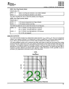
PCM1753
PCM1754
PCM1755
www.ti.com
SLES092A – OCTOBER 2003 – REVISED AUGUST 2004
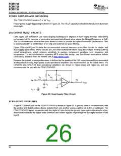
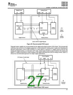
Digital Power
+V DGND
Analog Power
AGND +5VA +V
–V
S
D
S
V
CC
Digital Logic
and
Audio
Processor
Output
Circuits
DGND
PCM1753/54/55
AGND
Digital
Ground
Analog
Ground
Digital Section
Analog Section
Return Path for Digital Signals
Figure 30. Recommended PCB Layout
Separate power supplies are recommended for the digital and analog sections of the board. This prevents the
switching noise present on the digital supply from contaminating the analog power supply and degrading the
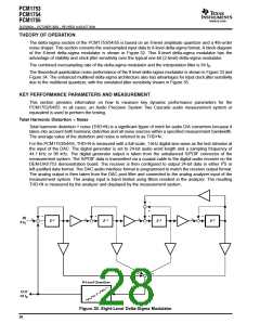
dynamic performance of the PCM1753/54/55. In cases where a common 5-V supply must be used for the
analog and digital sections, an inductance (RF choke, ferrite bead) should be placed between the analog and
digital 5-V supply connections to avoid coupling of the digital switching noise into the analog circuitry. Figure 31
shows the recommended approach for single-supply applications.
Power Supplies
RF Choke or Ferrite Bead
+5V AGND +V
–V
S
S
V
CC
V
DD
Output
Circuits
DGND
PCM1753/54/55
AGND
Common
Ground
Digital Section
Analog Section
Figure 31. Single-Supply PCB Layout
27

 BB [ BURR-BROWN CORPORATION ]