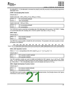
PCM1753
PCM1754
PCM1755
www.ti.com
SLES092A – OCTOBER 2003 – REVISED AUGUST 2004
SOFTWARE CONTROL (PCM1753/55)
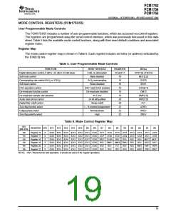
The PCM1753/55 has many programmable functions which can be controlled in the software control mode. The
functions are controlled by programming the internal registers using ML, MC, and MD.
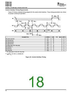
The serial control interface is a 3-wire serial port, which operates asynchronously to the audio serial interface.
The serial control interface is used to program the on-chip mode registers. The control interface includes MD
(pin 13), MC (pin 14), and ML (pin 15). MD is the serial data input, used to program the mode registers. MC
is the serial bit clock, used to shift data into the control port. ML is the control port latch clock.
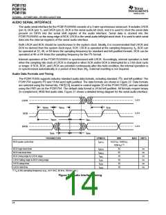
Register Write Operation
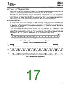
All write operations for the serial control port use 16-bit data words. Figure 23 shows the control data word
format. The most significant bit must be a 0. There are seven bits, labeled IDX[6:0], that set the register index
(or address) for the write operation. The least significant eight bits, D[7:0], contain the data to be written to the
register specified by IDX[6:0].
Figure 24 shows the functional timing diagram for writing to the serial control port. ML is held at a logic 1 state
until a register needs to be written. To start the register write cycle, ML is set to logic 0. Sixteen clocks are then
provided on MC, corresponding to the 16 bits of the control data word on MD. After the sixteenth clock cycle
has completed, ML is set to logic 1 to latch the data into the indexed mode control register.
LSB
D0
MSB
0
IDX6 IDX5 IDX4 IDX3 IDX2 IDX1 IDX0
D7
D6
D5
D4
D3
D2
D1
Register Index (or Address)
Register Data
Figure 23. Control Data Word Format for MD
ML
MC
MD
IDX6 IDX5 IDX4 IDX3 IDX2 IDX1 IDX0
IDX6
X
0
D7 D6 D5 D4
D3 D2 D1 D0
X
X
0
Figure 24. Register Write Operation
17

 BB [ BURR-BROWN CORPORATION ]