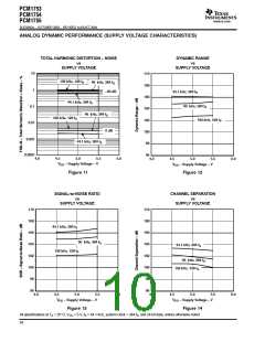
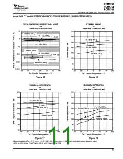
PCM1753
PCM1754
PCM1755
SLES092A – OCTOBER 2003 – REVISED AUGUST 2004
www.ti.com
AUDIO SERIAL INTERFACE
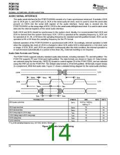
The audio serial interface for the PCM1753/54/55 consists of a 3-wire synchronous serial port. It includes LRCK
(pin 3), BCK (pin 1), and DATA (pin 2). BCK is the serial audio bit clock, and it is used to clock the serial data
present on DATA into the serial shift register of the audio interface. Serial data is clocked into the
PCM1753/54/55 on the rising edge of BCK. LRCK is the serial audio left/right word clock. It is used to latch serial
data into the internal registers of the serial audio interface.
Both LRCK and BCK should be synchronous to the system clock. Ideally, it is recommended that LRCK and
BCK be derived from the system clock input, SCK. LRCK is operated at the sampling frequency, f . BCK can
S
be operated at 32, 48, or 64 times the sampling frequency for standard and left-justified formats. BCK can be
2
operated at 48 or 64 times the sampling frequency for the I S format.
Internal operation of the PCM1753/54/55 is synchronized with LRCK. Accordingly, internal operation is held
when the sampling rate clock of LRCK is changed or when SCK and/or BCK is interrupted for a 3-bit clock cycle
or longer. If SCK, BCK, and LRCK are provided continuously after this held condition, the internal operation is
re-synchronized automatically in a period of less than 3/f . External resetting is not required.
S
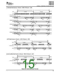
Audio Data Formats and Timing
2
The PCM1753/55 supports industry-standard audio data formats, including standard, I S, and left-justified. The
2
PCM1754 supports I S and 16-bit-word right-justified. The data formats are shown in Figure 22. Data formats
are selected using the format bits, FMT[2:0], located in control register 20 of the PCM1753/55, and are selected
using the FMT pin on the PCM1754. The default data format is 24-bit left-justified. All formats require binary
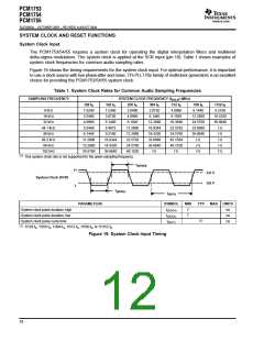
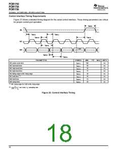
2s-complement, MSB-first audio data. Figure 21 shows a detailed timing diagram for the serial audio interface.
1.4 V
LRCK
t
t
(BCL)
t
(BCH)
(LB)
1.4 V
BCK
t
t
(BCY)
(BL)
1.4 V
DATA
t
t
(DS)
(DH)
PARAMETERS
SYMBOL
MIN
1/(32 f ), 1/(48 f ),
MAX UNITS
BCK pulse cycle time
t
(BCY)
S
S
(1)
1/(64 f )
S
BCK high-level time
t
35
35
10
10
10
10
ns
ns
ns
ns
ns
ns
(BCH)
BCK low-level time
t
(BCL)
BCK rising edge to LRCK edge
t
t
(BL)
(LB)
(DS)
(DH)
LRCK falling edge to BCK rising edge
DATA setup time
t
t
DATA hold time
(1)
f
S
is the sampling frequency (e.g., 44.1 kHZ, 48 kHz, 96 kHz, etc.).
Figure 21. Audio Interface Timing
14

 BB [ BURR-BROWN CORPORATION ]