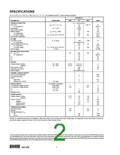
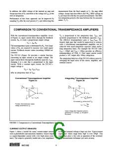
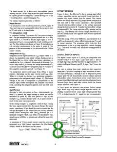
INPUT BIAS CURRENT ERRORS
CHOOSING CINT
Careful circuit board layout and assembly techniques are
required to achieve the very low input bias current capability
of the IVC102. The critical input connections are at ground
potential, so analog ground should be used as a circuit board
guard trace surrounding all critical nodes. These include
pins 2, 3, 4, 5 and 6. See Figure 4.
Internal capacitors C1, C2 and C3 are high quality metal/
oxide types with low leakage and excellent dielectric char-
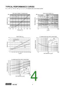
acteristics. Temperature stability is excellent—see typical
curve. They can be connected for CINT = 10pF, 30pF, 40pF,
60pF, 70pF, 90pF or 100pF. Connect unused internal ca-
pacitor pins to analog ground. Accuracy is ±20%, which
directly influences the gain of the transfer function.
Input bias current increases with temperature—see typical
performance curve Input Bias Current vs Temperature.
A larger value external CINT can be connected between pins
3 and 10 for slower/longer integration. Select a capacitor
type with low leakage and good temperature stability.
Teflon , polystyrene or polypropylene capacitors generally
provide excellent leakage, temperature drift and voltage
coefficient characteristics. Lower cost types such as NPO
ceramic, mica or glass may be adequate for many applica-
tions. Larger values for CINT require a longer reset time—see
typical curves.
HOLD MODE DROOP
Hold-mode droop is a slow change in output voltage prima-
rily due to op amp input bias current. Droop is specified
using the internal CINT = 100pF and is based on a –100fA
typical input bias current. Current flows out of the inverting
input of the internal op amp.
–100fA
Droop Rate =
CINT
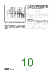
FREQUENCY RESPONSE
Integration of the input signal for a fixed period produces a
deep null (zero response) at the frequency 1/TINT and its
harmonics. An ac input current at this frequency (or its
harmonics) has zero average value and therefore produces
no output. This property can be used to position response
nulls at critical frequencies. For example, a 16.67ms integra-
tion period produces response nulls at 60Hz, 120Hz, 180Hz,
etc., which will reject ac line frequency noise and its har-
monics. Response nulls can be positioned to reduce interfer-
ence from system clocks or other periodic noise.
With CINT = 100pF, the droop rate is typically only
1nV/µs—slow enough that it rarely contributes significant
error at moderate temperatures.
Since the input bias current increases with temperature, the
droop rate will also increase with temperature. The droop
rate will approximately double for each 10°C increase in
junction temperature—see typical curves.
Droop rate is inversely proportional to CINT. If an external
integrator capacitor is used, a low leakage capacitor should
be selected to preserve the low droop performance of the
IVC102.
Response to all frequencies above f = 1/TINT falls at –20dB/
decade. The effective corner frequency of this single-pole
response is approximately 1/2.8TINT
.
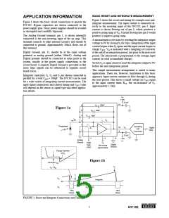
For the simple reset-and-integrate measurement technique,
TINT is equal to the to the time that S2 is open. The switched-
input technique, however, effectively integrates the input
signal throughout the full measurement cycle, including the
reset period and both hold periods. Using the timing shown
in Figure 3, the effective integration time is 1/Ts, where Ts
is the repetition rate of the sampling.
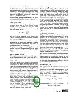
INPUT CURRENT RANGE
Extremely low input currents can be measured by integrat-
ing for long periods and/or using a small value for CINT
Input bias current of the internal op amp is the primary
source of error.
.
Larger input currents can be measured by increasing the
value of CINT and/or using a shorter integration time. Input
currents greater than 200µA should not be applied to the pin
2 input, however. The approximately 1.5kΩ series resistance
of S1 will create an input voltage at pin 2 that will begin to
forward-bias internal protection clamp diodes. Any current
that flows through these protection diodes will not be accu-
rately integrated. See “Input Impedance” section for more
information on input current-induced voltage.
INPUT IMPEDANCE
The input impedance of a perfect transimpedance circuit is
zero ohms. The input voltage ideally would be zero for any
input current. The actual input voltage when directly driving
the integrator input (pin 3) is proportional to the output slew
rate of the integrator. A 1V/µs slew rate produces approxi-
mately 100mV at pin 3. The input of the integrator can be
modeled as a resistance:
Input current greater than 200µA can, however, be con-
nected directly to pin 3, using the simple reset-integrate
technique shown in Figure 1. Current applied at this input
can be externally switched to avoid excessive I•R voltage
across S2 during reset. Inputs up to 5mA at pin 3 can be
accurately integrated if CINT is made large enough to limit
slew rate to less than 1V/µs. A 5mA input current would
require CINT = 5nF to produce a 1V/µs slew rate. The input
current appears as load current to the internal op amp,
reducing its ability to drive an external load.
RIN = 10–7/CINT
(2)
with RIN in Ω and CINT in Farads.
(3)
Using the internal CINT = C1 + C2 + C3 = 100pF
RIN = 10–7/100pF = 1kΩ
Teflon E. I. Du Pont de Nemours & Co.
®
9
IVC102

 BB [ BURR-BROWN CORPORATION ]