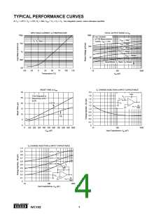
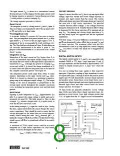
The input current, IIN, is shown as a conventional current
flowing into pin 2 in this diagram but the input current could
be bipolar (positive or negative). Current flowing out of pin
2 would produce a positive-ramping VO.
OFFSET ERRORS
Figure 3c shows the effect on VO due to op amp input offset
voltage, input bias current and switch charge injection. It
assumes zero input current from the sensor. The various
offsets and charge injection (∆Q) jumps shown are typical of
that seen with a 50pF source capacitance. The specified
“transfer function offset voltage” is the voltage measured
during the hold period at B. Transfer function offset voltage
is dominated by the charge injection of S2 opening and op
amp VOS. The opening and closing charge injections of S1
are very nearly equal and opposite and are not significant
contributors.
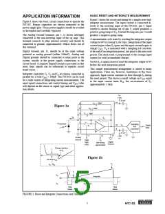
The timing sequence proceeds as follows:
Reset Period
The integrator is reset by closing switch S2 with S1 open. A
10µs reset time is recommended to allow the op amp to slew
to 0V and settle to its final value.
Pre-Integration Hold
S2 is opened, holding VO constant for 10µs prior to integra-
tion. This pre-integration hold period assures that S2 is fully
open before S1 is closed so that no input signal is lost. A
minimum of 1µs is recommended to avoid switching over-
lap. The 10µs hold period shown in Figure 3b also allows an
a/d converter measurement to be made at point A. The
purpose of this measurement at A is discussed in the “Offset
Errors” section.
Note that using a two-point difference measurement at A
and B can dramatically reduce offset due to op amp VOS and
S2 charge injection. The remaining offset with this B-A
measurement is due to op amp input bias current charging
CINT. This error is usually very small and is exaggerated in
the figure.
Integration on CINT
DIGITAL SWITCH INPUTS
Integration of the input current on CINT begins when S1 is
closed. An immediate step output voltage change occurs as
the charge that was stored on the input sensor capacitance is
transferred to CINT. Although this period of charging CINT
occurs only while S1 is closed, the charge transferred as S1
is closed causes the effective integration time to be equal to
the complete conversion period—see Figure 3b.
The digital control inputs to S1 and S2 are compatible with
standard CMOS or TTL logic. Logic input pins 11 and 12
are high impedance and the threshold is approximately 1.4V
relative to Digital Ground, pin 13. A logic “low” closes the
switch.
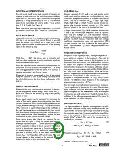
Use care in routing these logic signals to their respective
input pins. Capacitive coupling of logic transitions to sensi-
tive input nodes (pins 2 through 6) and to the positive power
supply (pin 14) will dramatically increase charge injection
and produce errors. Route these circuit board traces over a
ground plane (digital ground) and route digital ground traces
between logic traces and other critical traces for lowest
charge injection. See Figure 4.
The integration period could range from 100µs to many
minutes, depending on the input current and CINT value.
While S1 is closed, IIN charges CINT, producing a negative-
going ramp at the integrator output voltage, VO. The output
voltage at the end of integration is proportional to the
average input current throughout the complete conversion
cycle, including the integration period, reset and both hold
periods.
5V logic levels are generally satisfactory. Lower voltage
logic levels may help reduce charge injection errors, de-
pending on circuit layout. Logic high voltages greater than
5.5V, or higher than the V+ supply are not recommended.
Hold Period
Opening S1 halts integration on CINT. Approximately 5µs
after S1 is opened, the output voltage is stable and can be
measured (at point B). The hold period is 10µs in this
example. CINT remains charged until a S2 is again closed, to
reset for the next conversion cycle.
Analog
V+
Input trace guarded
all the way to sensor.
Ground
Switch logic inputs
guarded by digital
ground.
In this timing example, S1 is open for a total of 30µs. During
this time, signal current from the sensor charges the sensor
source capacitance. Care should be used to assure that the
voltage developed on the sensor does not exceed approxi-
mately 200mV during this time. The IIN terminal, pin 2, is
internally clamped with diodes. If these diodes forward bias,
signal current will flow to ground and will not be accurately
integrated.
1
14
•
•
•
•
•
•
•
•
•
•
•
•
•
•
Digital
Ground
•
S2
S1
Input nodes
guarded by
analog ground.
A maximum of 333nA signal current could be accurately
integrated on a 50pF sensor capacitance for 30µs before
200mV would be developed on the sensor.
7
8
VO
IMAX = (50pF) (200mV)/30µs = 333nA
Pins 7 and 8 have no internal
connection but are connected to
ground for lowest noise pickup.
V–
FIGURE 4. Circuit Board Layout Techniques.
®
8
IVC102

 BB [ BURR-BROWN CORPORATION ]