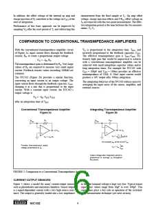
In addition, the offset voltage of the internal op amp and
charge injection of S2 contribute to the voltage on CINT at the
start of integration.
measurement from the final sample at T2. Op amp offset
voltage, charge injection effects and I•RS2 offset voltage on
S2 are removed with this two-point measurement. The effec-
tive integration period is the time between the two measure-
ments, T2-T1.
Performance of this basic approach can be improved by
sampling VO after the reset period at T1 and subtracting this
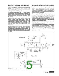
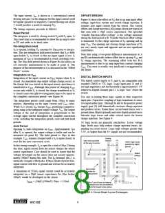
COMPARISON TO CONVENTIONAL TRANSIMPEDANCE AMPLIFIERS
With the conventional transimpedance amplifier circuit
of Figure 2a, input current flows through the feedback
resistor, RF, to create a proportional output voltage.
VO is proportional to the integration time, TINT, and
inversely proportional to the feedback capacitor, CINT
.
The effective transimpedance gain is TINT /CINT. Ex-
tremely high gain that would be impractical to achieve
with a conventional transimpedance amplifier can be
achieved with small integration capacitor values and/or
long integration times. For example the IVC102 with
CINT = 100pF and TINT = 100ms provides an effective
transimpedance of 1GΩ. A 10nA input current would
produce a 10V output after 100ms integration.
VO = –IIN RF
The transimpedance gain is determined by RF. Very large
values of RF are required to measure very small signal
current. Feedback resistor values exceeding 100MΩ are
common.
The IVC102 (Figure 2b) provides a similar function,
converting an input current to an output voltage. The
The integrating behavior of the IVC102 reduces noise by
averaging the input noise of the sensor, amplifier, and
external sources.
input current flows through the feedback capacitor, CINT
,
charging it at a rate that is proportional to the input
current. With a constant input current, the IVC102’s
output voltage is
VO = –IIN TINT/CINT
after an integration time of TINT
.
Conventional Transimpedance Amplifier
Figure 2a
Integrating Transimpedance Amplifier
Figure 2b
IIN
IIN
CINT
RF
VO
VO
–1
VO
=
CINT
IIN(t) dt
VO = –IIN RF
∫
for constant IIN, at the end of TINT
Provides time-continuous output
TINT
VO = –IIN
CINT
voltage proportional to IIN
.
Output voltage after integration period is
proportional to average IIN throughout
the period.
FIGURE 2. Comparison to a Conventional Transimpedance Amplifier.
CURRENT-OUTPUT SENSORS
Figure 3 shows a model for many current-output sensors
such as photodiodes and ionization chambers. Sensor output
is a signal-dependent current with a very high source resis-
tance. The output is generally loaded into a low impedance
so that the terminal voltage is kept very low. Typical sensor
capacitance values range from 10pF to over 100pF. This
capacitance plays a key role in operation of the switched-
input measurement technique (see next section).
®
6
IVC102

 BB [ BURR-BROWN CORPORATION ]