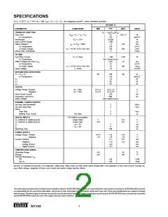
SPECIFICATIONS
At TA = +25°C, VS = ±15V, RL = 2kΩ, CINT = C1 + C2 + C3, 1ms integration period(1), unless otherwise specified.
IVC102P, U
PARAMETER
CONDITIONS
MIN
TYP
MAX
UNITS
TRANSFER FUNCTION
Gain Error
vs Temperature
Nonlinearity
Input Current Range
Offset Voltage(2)
vs Temperature
vs Power Supply
Droop Rate, Hold Mode
VO = –(IIN)(TINT)/CINT
CINT = C1 + C2 + C3
±5
±25
±0.005
±100
–5
±30
150
–1
+25/–17
%
ppm/°C
%
µA
mV
µV/°C
µV/V
nV/µs
V
O = ±10V
IIN = 0, C = 50pF
±20
IN
VS = +4.75/–10 to +18/–18V
750
OP AMP
Input Bias Current
vs Temperature
Offset Voltage (Op Amp VOS
vs Temperature
vs Power Supply
Noise Voltage
S1, S2 Open
–100
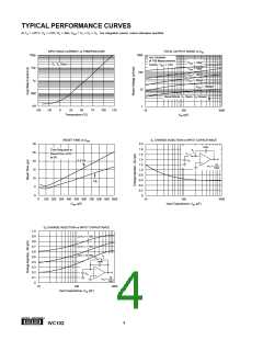
See Typical Curve
±750
±5
fA
)
±0.5
±5
10
mV
µV/°C
µV/V
VS = +4.75/–10 to +18/–18V
f = 1kHz
100
10
nV/√Hz
INTEGRATION CAPACITORS
C1 + C2 + C3
80
100
±25
10
30
60
120
pF
ppm/°C
pF
pF
pF
vs Temperature
C1
C2
C3
OUTPUT
Voltage Range, Positive
Negative
RL = 2kΩ
RL = 2kΩ
(V+)–3
(V–)+3
(V+)–1.3
(V–)+2.6
V
V
Short-Circuit Current
Capacitive Load Drive
Noise Voltage
±20
500
mA
pF
See Typical Curve
DYNAMIC CHARACTERISTIC
Op Amp Gain-Bandwidth
Op Amp Slew Rate
Reset
2
3
MHz
V/µs
Slew Rate
Settling Time, 0.01%
3
6
V/µs
µs
10V Step
DIGITAL INPUTS
(TTL/CMOS Compatible)
(Logic High)
(Logic Low)
V
IH (referred to digital ground)
2
–0.5
5.5
0.8
V
V
VIL (referred to digital ground)
IIH
IIL
VIH = 5V
VIL = 0V
2
0
100
µA
µA
ns
Switching Time
POWER SUPPLY
Voltage Range: Positive
Negative
Current: Positive
Negative
+4.75
–10
+15
–15
4.1
–1.6
–0.2
–2.3
+18
–18
5.5
V
V
mA
mA
mA
mA
–2.2
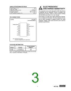
Analog Ground
Digital Ground
TEMPERATURE RANGE
Operating Range
Storage
–40
–55
85
125
°C
°C
Thermal Resistance, θJA
DIP
100
150
°C/W
°C/W
SO-14
NOTES: (1) Standard test timing: 1ms integration, 200µs hold, 100µs reset. (2) Hold mode output voltage after 1ms integration of zero input current. Includes op
amp offset voltage, integration of input error current and switch charge injection effects.
The information provided herein is believed to be reliable; however, BURR-BROWN assumes no responsibility for inaccuracies or omissions. BURR-BROWN assumes
no responsibility for the use of this information, and all use of such information shall be entirely at the user’s own risk. Prices and specifications are subject to change
without notice. No patent rights or licenses to any of the circuits described herein are implied or granted to any third party. BURR-BROWN does not authorize or warrant
any BURR-BROWN product for use in life support devices and/or systems.
®
2
IVC102

 BB [ BURR-BROWN CORPORATION ]