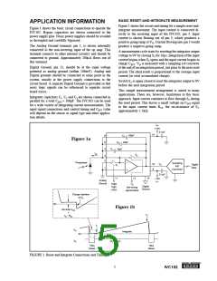
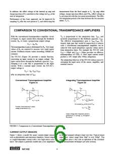
BASIC RESET-AND-INTEGRATE MEASUREMENT
APPLICATION INFORMATION
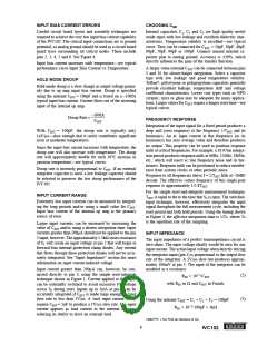
Figure 1 shows the circuit and timing for a simple reset-and-
integrate measurement. The input current is connected di-
rectly to the inverting input of the IVC102, pin 3. Input
current is shown flowing out of pin 3, which produces a
positive-going ramp at VO. Current flowing into pin 3 would
produce a negative-going ramp.
Figure 1 shows the basic circuit connections to operate the
IVC102. Bypass capacitors are shown connected to the
power supply pins. Noisy power supplies should be avoided
or decoupled and carefully bypassed.
The Analog Ground terminal, pin 1, is shown internally
connected to the non-inverting input of the op amp. This
terminal connects to other internal circuitry and should be
connected to ground. Approximately 200µA flows out of
this terminal.
A measurement cycle starts by resetting the integrator output
voltage to 0V by closing S2 for 10µs. Integration of the input
current begins when S2 opens and the input current begins to
charge CINT. VO is measured with a sampling a/d converter
at the end of an integration period, just prior to the next reset
period. The ideal result is proportional to the average input
current (or total accumulated charge).
Digital Ground, pin 13, should be at the same voltage
potential as analog ground (within 100mV). Analog and
Digital grounds should be connected at some point in the
system, usually at the power supply connections to the
circuit board. A separate Digital Ground is provided so that
noisy logic signals can be referenced to separate circuit
board traces.
Switch S2 is again closed to reset the integrator output to 0V
before the next integration period.
This simple measurement arrangement is suited to many
applications. There are, however, limitations to this basic
approach. Input current continues to flow through S2 during
the reset period. This leaves a small voltage on CINT equal
to the input current times RS2, the on-resistance of S2,
approximately 1.5kΩ.
Integrator capacitors C1, C2 and C3 are shown connected in
parallel for a total CINT = 100pF. The IVC102 can be used
for a wide variety of integrating current measurements. The
input signal connections and control timing and CINT value
will depend on the sensor or signal type and other applica-
tion details.
V+
+15V
0.1µF
14
C3
30pF
60pF
6
Figure 1a
C2
10pF
5
4
C1
IIN
S2
3
2
Photodiode
Sampling
A/D
Converter
10
9
VO
Digital
Data
S1
1
0.1µF
11
12
S2
13
–15V
V–
Analog
Ground
Logic
High
(+5V)
Digital
Ground
See timing
signal below
Charge Injection
of S2
0V
Figure 1b
Op Amp VOS
+
T2
IIN • RS2
T1
VO
0V
Integrate
S2
(S2 Open)
10µs
Reset
10µs
Reset
FIGURE 1. Reset-and Integrate Connections and Timing.
®
5
IVC102

 BB [ BURR-BROWN CORPORATION ]