V+
+15V
0.1µF
14
C3
60pF
6
5
4
3a
C2
10pF
30pF
C1
S2
Photodiode
Sensor
3
2
10
9
VO
I
R
C
Digital
Data
A/D
Converter
S1
1
0.1µF
11
S1
12
S2
13
–15V
V–
I: Signal - Dependent Current
R: Sensor Resistance
C: Sensor Capacitance
See timing
signals below
Effective
Signal Integration
Period, TS
A
3b
0V
0V
VO waveform with
approx. half-scale input current.
Charge transferred
from sensor C
VO
B
to CINT
.
(S1 Open)
(S1 Closed)
(S2 Open)
S1
S2
10µs
10µs
10µs
10µs
10µs
Hold Reset Pre-Int.
Hold
Hold Reset
+10mV
VO waveform with
zero input current.
Op Amp
VOS
Transfer Function
Offset Voltage
3c
0V
VO
0V
A
Ramp due to
input bias current
(exaggerated).
∆Q
S1 Closing
∆Q
S1 Opening
–10mV
∆Q
S2 Opening
B
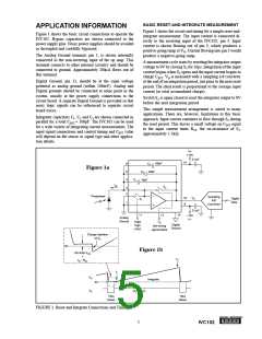
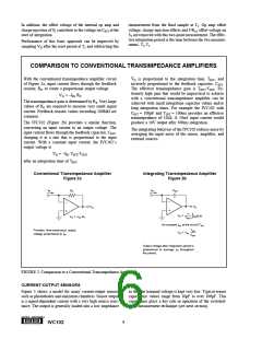
FIGURE 3. Switched-Input Measurement Technique.
SWITCHED-INPUT MEASUREMENT TECHNIQUE
Input connections and timing are shown in Figure 3.
While the basic reset-and-integrate measurement arrange-
ment in Figure 1 is satisfactory for many applications, the
switched-input timing technique shown in Figure 3 has
important advantages. This method can provide continuous
integration of the input signal. Furthermore, it can hold the
output voltage constant after integration for stable conver-
sion (desirable for a/d converter without a sample/hold).
The timing diagram, Figure 3b, shows that S1 is closed only
when S2 is open. During the short period that S1 is open
(30µs in this timing example), any signal current produced
by the sensor will charge the sensor’s source capacitance.
This charge is then transferred to CINT when S1 is closed. As
a result, no charge produced by the sensor is lost and the
input signal is continuously integrated. Even fast input
pulses are accurately integrated.
®
7
IVC102

 BB [ BURR-BROWN CORPORATION ]