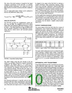
GROUNDING, DECOUPLING, AND
LAYOUT INFORMATION
Low noise is required for all supply and ground connections
to the DAC2902. It is recommended to use a multilayer PCB
utilizing separate power and ground planes. Mixed signal
designs require particular attention to the routing of the
different supply currents and signal traces. Generally, analog
supply and ground planes should only extend into analog
signal areas, such as the DAC output signal and the refer-
ence signal. Digital supply and ground planes must be
confined to areas covering digital circuitry, including the
digital input lines connecting to the converter, as well as the
clock signal. The analog and digital ground planes should be
joined together at one point underneath the DAC. This can
be realized with a short track of approximately 1/8" (3mm).
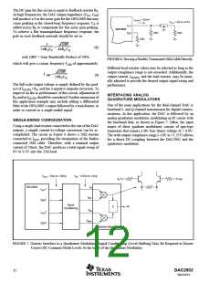
Proper grounding and bypassing, short lead length, and the use
of ground planes are particularly important for high-frequency
designs. Multilayer PCBs are recommended for best perfor-
mance since they offer distinct advantages such as minimiza-
tion of ground impedance, separation of signal layers by
ground layers, etc.
The DAC2902 uses separate pins for its analog and digital
supply and ground connections. The placement of the decou-
pling capacitor should be such that the analog supply (+VA)
is bypassed to the analog ground (AGND), and the digital
supply bypassed to the digital ground (DGND). In most
cases 0.1µF ceramic chip capacitors at each supply pin are
adequate to provide a low impedance decoupling path. Keep
in mind that their effectiveness largely depends on the
proximity to the individual supply and ground pins. There-
fore, they should be located as close as physically possible
to those device leads. Whenever possible, the capacitors
should be located immediately under each pair of supply/
ground pins on the reverse side of the pc board. This layout
approach will minimize the parasitic inductance of compo-
nent leads and PCB runs.
The power to the DAC2902 should be provided through the
use of wide PCB runs or planes. Wide runs will present a
lower trace impedance, further optimizing the supply decou-
pling. The analog and digital supplies for the converter
should only be connected together at the supply connector of
the pc board. In the case of only one supply voltage being
available to power the DAC, ferrite beads along with bypass
capacitors may be used to create an LC filter. This will
generate a low-noise analog supply voltage that can then be
connected to the +VA supply pin of the DAC2902.
While designing the layout, it is important to keep the analog
signal traces separated from any digital line, in order to
prevent noise coupling onto the analog signal path.
Further supply decoupling with surface-mount tantalum ca-
pacitors (1µF to 4.7µF) may be added as needed in proxim-
ity of the converter.
DAC2902
SBAS167A
15

 BB [ BURR-BROWN CORPORATION ]