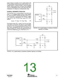
As shown in Figure 3, the transformer’s center tap is con-
nected to ground. This forces the voltage swing on IOUT and
IOUT to be centered at 0V. In this case the two resistors, RL,
may be replaced with one, RDIFF, or omitted altogether. This
approach should only be used if all components are close to
each other, and if the VSWR is not important. A complete
power transfer from the DAC output to the load can be
realized, but the output compliance range should be ob-
served. Alternatively, if the center tap is not connected, the
signal swing will be centered at RL • IOUTFS/2. However, in
this case, the two resistors (RL) must be used to enable the
necessary DC-current flow for both outputs.
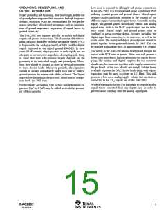
The OPA680 is configured for a gain of two. Therefore,
operating the DAC2902 with a 20mA full-scale output will
produce a voltage output of ±1V. This requires the amplifier
to operate off of a dual power supply (±5V). The tolerance
of the resistors typically sets the limit for the achievable
common-mode rejection. An improvement can be obtained
by fine tuning resistor R4.
This configuration typically delivers a lower level of ac
performance than the previously discussed transformer solu-
tion because the amplifier introduces another source of dis-
tortion. Suitable amplifiers should be selected based on their
slew-rate, harmonic distortion, and output swing capabilities.
High-speed amplifiers like the OPA680 or OPA687 may be
considered. The ac performance of this circuit may be im-
proved by adding a small capacitor (CDIFF) between the
outputs IOUT and IOUT, as shown in Figure 4). This will
introduce a real pole to create a low-pass filter in order to
slew-limit the DAC’s fast output signal steps, that otherwise
could drive the amplifier into slew-limitations or into an
overload condition; both would cause excessive distortion.
The difference amplifier can easily be modified to add a level
shift for applications requiring the single-ended output volt-
age to be unipolar, i.e., swing between 0V and +2V.
ADTT1-1
(Mini-Circuits)
1:1
IOUT
RL
50Ω
RS
RDIFF
DAC2902
50Ω
100Ω
IOUT
RL
50Ω
DUAL TRANSIMPEDANCE OUTPUT CONFIGURATION
FIGURE 3. Differential Output Configuration Using an RF
Transformer.
The circuit example of Figure 5 shows the signal output
currents connected into the summing junctions of the dual
voltage-feedback op amp OPA2680 that is set up as a
transimpedance stage, or ‘I-to-V converter’. With this cir-
cuit, the DAC’s output will be kept at a virtual ground,
minimizing the effects of output impedance variations, which
results in the best DC linearity (INL). As mentioned previ-
ously, care should be taken not to drive the amplifier into
slew-rate limitations, and produce unwanted distortion.
DIFFERENTIAL CONFIGURATION USING AN OP AMP
If the application requires a DC-coupled output, a difference
amplifier may be considered, as shown in Figure 4. Four
external resistors are needed to configure the voltage-feed-
back op amp OPA680 as a difference amplifier performing
the differential to single-ended conversion. Under the shown
configuration, the DAC2902 generates a differential output
signal of 0.5Vp-p at the load resistors, RL. The resistor
values shown were selected to result in a symmetric 25Ω
loading for each of the current outputs since the input
impedance of the difference amplifier is in parallel to resis-
tors RL, and should be considered.
+5V
50Ω
1/2
OPA2680
–VOUT = IOUT • RF1
RF1
CF1
DAC2902
R2
402Ω
IOUT
CD1
R1
200Ω
RF2
CF2
IOUT
VOUT
DAC2902
OPA680
IOUT
CD2
IOUT
R3
200Ω
COPT
–5V +5V
1/2
OPA2680
RL
28.7Ω
R4
402Ω
RL
26.1Ω
–VOUT = IOUT • RF2
50Ω
–5V
FIGURE 4. Difference Amplifier Provides Differential to
Single-Ended Conversion and DC-Coupling.
FIGURE 5. Dual, Voltage-Feedback Amplifier OPA2680
Forms Differential Transimpedance Amplifier.
DAC2902
SBAS167A
11

 BB [ BURR-BROWN CORPORATION ]