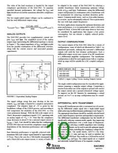
one RSET connected to the FSA1 pin (pin 44) and the other to
the FSA2 pin (pin 41). In this configuration, the user has the
flexibility to set and adjust the full-scale output current for each
DAC independently, allowing for the compensation of possible
gain mismatches elsewhere within the transmit signal path.
+5V
+VA
DAC2902
VREF
RSET
Alternatively, bringing the GSET pin HIGH (i.e. connected to
+VA), the DAC2902 will switch into the simultaneous gain set
mode. Now the full-scale output current of both DAC chan-
nels is determined by only one external RSET resistor con-
nected to the FSA1 pin. The resistor at the FSA2 pin may be
removed, however this is not required since this pin is not
functional in this mode and the resistor has no effect to the
gain equation. The formula for deriving the correct RSET
remains unchanged, e.g. RSET = 2ký will result in a 20mA
output for both DACs.
IREF
=
FSA
Ref
Current
Sources
Control
Amp
REFIN
RSET
2kΩ
0.1µF
+1.25V Ref.
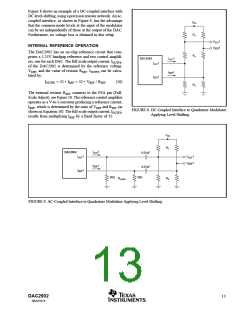
EXTERNAL REFERENCE OPERATION
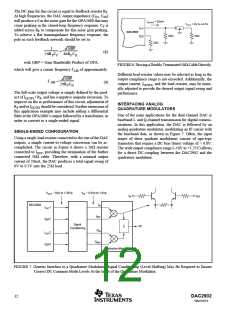
FIGURE 10. Internal Reference Configuration.
The internal reference can be disabled by simply applying an
external reference voltage into the REFIN pin, which in this
case functions as an input, as shown in Figure 11. The use
of an external reference may be considered for applications
that require higher accuracy and drift performance, or to add
the ability of dynamic gain control.
Using the internal reference, a 2kΩ resistor value results in
a full-scale output of approximately 20mA. Resistors with a
tolerance of 1% or better should be considered. Selecting
higher values, the output current can be adjusted from 20mA
down to 2mA. Operating the DAC2902 at lower than 20mA
output currents may be desirable for reasons of reducing the
total power consumption, optimizing the distortion perfor-
mance, or observing the output compliance voltage limita-
tions for a given load condition.
While a 0.1µF capacitor is recommended to be used with the
internal reference, it is optional for the external reference
operation. The reference input, REFIN, has a high input
impedance (1MΩ) and can easily be driven by various
sources. Note that the voltage range of the external reference
should stay within the compliance range of the reference
input (0.5V to 1.25V).
It is recommended to bypass the REFIN pin with a ceramic
chip capacitor of 0.1µF or more. The control amplifier is
internally compensated, and its small signal bandwidth is
approximately 0.3MHz.
POWER-DOWN MODE
The DAC2902 features a power-down function that can be
used to reduce the total supply current to less than 6mA.
Applying a logic HIGH to the PD pin will initiate the power-
down mode, while a logic LOW enables normal operation.
When left unconnected, an internal active pull-down circuit
will enable the normal operation of the converter.
GAIN SETTING OPTIONS
The full-scale output current on the DAC2902 can be set two
ways: either for each of the two DAC channels independently
or for both channels simultaneously. For the independent gain
set mode, the GSET pin (pin 42) must be LOW (i.e. connected
to AGND). In this mode, two external resistors are required—
+5V
+VA
DAC2902
VREF
IREF
=
RSET
FSA
Ref
Control
Amp
Current
Sources
REFIN
External
Reference
RSET
+1.25V Ref.
FIGURE 11. External Reference Configuration.
14
DAC2902
SBAS167A

 BB [ BURR-BROWN CORPORATION ]