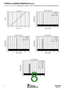
The DC gain for this circuit is equal to feedback resistor RF.
At high frequencies, the DAC output impedance (CD1, CD2)
will produce a 0 in the noise gain for the OPA2680 that may
cause peaking in the closed-loop frequency response. CF is
added across RF to compensate for this noise gain peaking.
To achieve a flat transimpedance frequency response, the
pole in each feedback network should be set to:
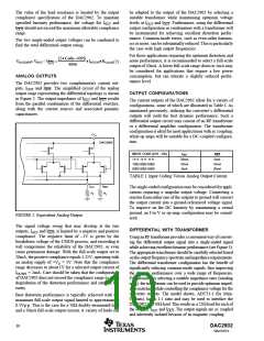
IOUTFS = 20mA
VOUT = 0V to +0.5V
IOUT
DAC2902
IOUT
50Ω
50Ω
25Ω
1
GBP
=
(8)
2πRFCF 4πRF CD
with GBP = Gain Bandwidth Product of OPA,
FIGURE 6. Driving a Doubly Terminated 50Ω Cable Directly.
which will give a corner frequency f-3dB of approximately:
Different load resistor values may be selected as long as the
output compliance range is not exceeded. Additionally, the
output current, IOUTFS, and the load resistor, may be mutu-
ally adjusted to provide the desired output signal swing and
performance.
GBP
f−3dB
=
(9)
2πRFCD
The full-scale output voltage is simply defined by the prod-
uct of IOUTFS • RF, and has a negative unipolar excursion. To
improve on the ac performance of this circuit, adjustment of
RF and/or IOUTFS should be considered. Further extensions of
this application example may include adding a differential
filter at the OPA2680’s output followed by a transformer, in
order to convert to a single-ended signal.
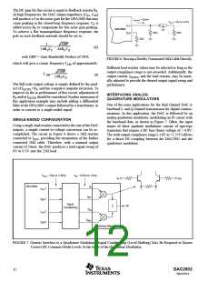
INTERFACING ANALOG
QUADRATURE MODULATORS
One of the main applications for the dual-channel DAC is
baseband I- and Q-channel transmission for digital commu-
nications. In this application, the DAC is followed by an
analog quadrature modulator, modulating an IF carrier with
the baseband data, as shown in Figure 7. Often, the input
stages of these quadrate modulators consist of npn-type
transistors that require a DC bias (base) voltage of > 0.8V.
The wide output compliance range (–10V to +1.25V) allows
for a direct DC–coupling between the DAC2902 and the
quadrature modulator.
SINGLE-ENDED CONFIGURATION
Using a single-load resistor connected to the one of the DAC
outputs, a simple current-to-voltage conversion can be ac-
complished. The circuit in Figure 6 shows a 50Ω resistor
connected to IOUT, providing the termination of the further
connected 50Ω cable. Therefore, with a nominal output
current of 20mA, the DAC produces a total signal swing of
0V to 0.5V into the 25Ω load.
VOUT ~ 0Vp to 1.20Vp
VIN ~ 0.6Vp to 1.8Vp
IIN
IREF
IIN
DAC2902
IOUT
1
IREF
I
OUT1
Signal
Conditioning
∑
RF
QIN
IOUT
2
QREF
I
OUT2
Quadrature Modulator
FIGURE 7. Generic Interface to a Quadrature Modulator. Signal Conditioning (Level-Shifting) May Be Required to Ensure
Correct DC Common-Mode Levels At the Input of the Quadrature Modulator.
DAC2902
SBAS167A
12

 BB [ BURR-BROWN CORPORATION ]