DAC TRANSFER FUNCTION
APPLICATION INFORMATION
THEORY OF OPERATION
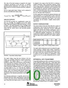
Each of the DACs in the DAC2902 has a complementary
current output, IOUT1 and IOUT2. The full-scale output cur-
rent, IOUTFS, is the summation of the two complementary
output currents:
The architecture of the DAC2902 uses the current steering
technique to enable fast switching and a high update rate.
The core element within the monolithic DAC is an array of
segmented current sources that are designed to deliver a full-
scale output current of up to 20mA, as shown in Figure 1. An
internal decoder addresses the differential current switches
each time the DAC is updated and a corresponding output
current is formed by steering all currents to either output
summing node, IOUT or IOUT. The complementary outputs
deliver a differential output signal, which improves the
dynamic performance through reduction of even-order har-
monics, common-mode signals (noise), and double the peak-
to-peak output signal swing by a factor of two, compared to
single-ended operation.
IOUTFS = IOUT + IOUT
(1)
The individual output currents depend on the DAC code and
can be expressed as:
IOUT = IOUTFS • (Code/4096)
IOUT = IOUTFS • (4095 - Code)
(2)
(3)
where ‘Code’ is the decimal representation of the DAC data
input word. Additionally, IOUTFS is a function of the refer-
ence current IREF, which is determined by the reference
The segmented architecture results in a significant reduction
of the glitch energy, improves the dynamic performance
(SFDR), and DNL. The current outputs maintain a very high
output impedance of greater than 200ký.
voltage and the external setting resistor, RSET
.
The full-scale output current is determined by the ratio of the
internal reference voltage (approx. +1.25V) and an external
resistor, RSET. The resulting IREF is internally multiplied by a
factor of 32 to produce an effective DAC output current that
IOUTFS = 32 • IREF = 32 • VREF/RSET
(4)
In most cases the complementary outputs will drive resistive
loads or a terminated transformer. A signal voltage will
develop at each output according to:
can range from 2mA to 20mA, depending on the value of RSET
.
The DAC2902 is split into a digital and an analog portion,
each of which is powered through its own supply pin. The
digital section includes edge-triggered input latches and the
decoder logic, while the analog section comprises the cur-
rent source array with its associated switches, and the
reference circuitry.
VOUT = IOUT • RLOAD
VOUT = IOUT • RLOAD
(5)
(6)
+VD
+VD
+VA
lOUT
1
Data Input
Port 1
D[11:0]_1
DAC1
Segmented Switches
Current Sources
Input
Latch 1
DAC
Latch 1
lOUT1
REFIN
WRT1
CLK1
CLK2
WRT2
FSA1
FSA2
GSET
PD
Reference
Control Amplifier
DAC2902
lOUT
2
Data Input
Port 2
D[11:0]_2
DAC2
Segmented Switches
Current Sources
Input
Latch 2
DAC
Latch 2
lOUT2
DGND
DGND
AGND
FIGURE 1. Block Diagram of the DAC2902.
DAC2902
SBAS167A
9

 BB [ BURR-BROWN CORPORATION ]