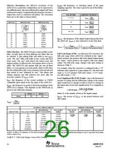
Effective Resolution—the effective resolution of the
ADS1218 in a particular configuration can be expressed in
two different units: bits rms (referenced to output) and Vrms
(referenced to input). Computed directly from the converter’s
output data, each is a statistical calculation. The conversion
from one to the other is shown below.
fSAMP—the frequency, or switching speed, of the input
sampling capacitor. The value is given by one of the follow-
ing equations:
PGA SETTING
SAMPLING FREQUENCY
fOSC
1, 2, 4, 8
fSAMP
fSAMP
fSAMP
=
=
=
mfactor
OSC • 2
mfactor
OSC • 4
mfactor
f
16
32
BITS rms
BIPOLAR Vrms
UNIPOLAR Vrms
2 • VREF
VREF
f
PGA
6.02•ER
PGA
6.02•ER
20
20
f
OSC • 8
10
10
64, 128
fSAMP
=
mfactor
24
22
20
18
16
14
12
298nV
1.19µV
4.77µV
19.1µV
76.4µV
505µV
1.22mV
149nV
597nV
2.39µV
9.55µV
38.2µV
152.7µV
610µV
fDATA—the frequency of the digital output data produced by
the ADS1218, fDATA is also referred to as the Data Rate.
fMOD
fOSC
fDATA
=
=
Decimation Ratio
mfactor • Decimation Ratio
Filter Selection—the ADS1218 uses a (sinx /x) filter or sinc
filter. Actually there are three different sinc filters that can
be selected. A fast settling filter will settle in one tDATA
cycle. The sinc2 filter will settle in two cycles and have
lower noise. The sinc3 will achieve the lowest noise and
highest number of effective bits, but requires three cycles to
settle. The ADS1218 will operate with any one of these
filters, or it can operate in an auto mode, where it will select
the fast settling filter after a new channel is selected and will
then switch to sinc2 followed by sinc3. This allows fast
settling response and still achieves low noise after the
necessary number of tDATA cycles.
Full-Scale Range (FSR)—as with most A/D converters, the
full-scale range of the ADS1218 is defined as the “input”,
which produces the positive full-scale digital output minus
the “input”, which produces the negative full-scale digital
output. The full-scale range changes with gain setting as
shown in Table V.
For example, when the converter is configured with a 2.5V
reference and is placed in a gain setting of 2, the full-scale
range is: [1.25V (positive full-scale) minus –1.25V (nega-
tive full-scale)] = 2.5V.
Least Significant Bit (LSB) Weight—this is the theoretical
amount of voltage that the differential voltage at the analog
input would have to change in order to observe a change in
the output data of one least significant bit. It is computed as
follows:
fOSC—the frequency of the crystal oscillator or CMOS
compatible input signal at the XIN input of the ADS1218.
fMOD—the frequency or speed at which the modulator of the
ADS1218 is running. This depends on the SPEED bit as
given by the following equation:
Full
−
Scale Range
2N
LSB Weight =
where N is the number of bits in the digital output.
DATA—the inverse of fDATA, or the period between each
data output.
SPEED = 0
SPEED = 1
mfactor
128
256
t
fOSC
mfactor
fMOD
=
5V SUPPLY ANALOG INPUT(1)
GENERAL EQUATIONS
DIFFERENTIAL
FULL-SCALE RANGE INPUT VOLTAGES(2)
PGA OFFSET
FULL-SCALE
RANGE
DIFFERENTIAL
INPUT VOLTAGES(2)
PGA SHIFT
RANGE
GAIN SETTING
RANGE
2 • VREF
±VREF
±VREF
1
2
5V
±2.5V
±1.25V
±0.625V
PGA
PGA
2 • PGA
2.5V
±1.25V
4
1.25V
±0.625V
±312.5mV
±156.25mV
±78.125mV
±39.0625mV
±19.531mV
±9.766mV
8
0.625V
±312.5mV
±156.25mV
±78.125mV
±39.0625mV
±19.531mV
16
32
64
128
312.5mV
156.25mV
78.125mV
39.0625mV
NOTES: (1) With a 2.5V reference. (2) The ADS1218 allows common-mode voltage as long as the absolute input voltage on AINP or AINN does not go below
AGND or above AVDD
.
TABLE V. Full-Scale Range versus PGA Setting.
ADS1218
26
SBAS187

 BB [ BURR-BROWN CORPORATION ]