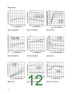
Switching Specifications (AC)
Unless otherwise noted, all typical values at T = 25°C, V
= 5 V, and V
- V = 30 V, V - V = 0 V;
EE E EE
A
CC1
CC2
all Minimum/Maximum specifications are at Recommended Operating Conditions.
Parameter
Symbol
Min. Typ.
Max. Units
Test Conditions
Fig.
Note
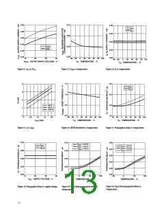
VIN to High Level Output
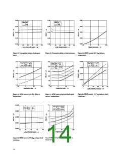
Propagation Delay Time
tPLH
0.10
0.30
0.50 µs
Rg = 10 Ω
Cg = 10 nF,
17,18,19, 15
20,21,22,
f = 10 kHz,
Duty Cycle = 50%
45,54,55
VIN to Low Level Output
Propagation Delay Time
tPHL
0.10
0.32
0.50
Pulse Width Distortion
PWD
-0.30 0.02
-0.35
0.30
0.35
16,17
Propagation Delay Difference
Between Any Two Parts
(tPHL - tPLH
PDD
)
17,18
10% to 90% Rise Time
tr
tf
0.1
0.1
0.3
45
90% to 10% Fall Time
DESAT Sense to 90% VOUT Delay
tDESAT(90%)
tDESAT(10%)
tDESAT(FAULT)
tDESAT(LOW)
tRESET(FAULT)
0.5
3.0
5
Rg = 10 Ω,
Cg = 10 nF
23,56
19
DESAT Sense to 10% VOUT Delay
2.0
VCC2 - VEE = 30 V
24,28,
46,56
DESAT Sense to Low Level FAULT
Signal Delay
1.8
25,47,
56
20
21
22
DESAT Sense to DESAT Low
Propagation Delay
0.25
56
RESET to High Level FAULT Signal
Delay
3
7
20
26,27,
56
RESET Signal Pulse Width
UVLO to VOUT High Delay
UVLO to VOUT Low Delay
PWRESET
tUVLO ON
tUVLO OFF
|CMH|
0.1
4.0
6.0
30
VCC2 = 1.0 ms
ramp
49
13
14
23
Output High Level Common Mode
Transient Immunity
15
15
kV/µs TA = 25°C,
50,51,
52,53
VCM = 1500 V,
VCC2 = 30 V
Output Low Level Common Mode
Transient Immunity
|CML|
30
TA = 25°C,
VCM = 1500 V,
VCC2 = 30 V
24
10

 AVAGO [ AVAGO TECHNOLOGIES LIMITED ]