Notes:
1. Bypassing of the power supply line is required, with a 0.1 µF ceramic disc capacitor adjacent to each optocoupler as illustrated in Figure 15. Total
lead length between both ends of the capacitor and the isolator pins should not exceed 20 mm.
2. Device considered a two terminal device: pins 1, 2, 3, and 4 shorted together, and pins 5, 6, 7, and 8 shorted together.
3. The tPLH propagation delay is measured from the 3.75 mA point on the falling edge of the input pulse to the 1.5 V point on the rising edge of the
output pulse.
4. The tPHL propagation delay is measured from the 3.75 mA point on the rising edge of the input pulse to the 1.5 V point on the falling edge of the
output pulse.
5. The tELH enable propagation delay is measured from the 1.5 V point on the falling edge of the enable input pulse to the 1.5 V point on the rising edge
of the output pulse.
6. The tEHL enable propagation delay is measured from the 1.5 V point on the rising edge of the enable input pulse to the 1.5 V point on the falling edge
of the output pulse.
7. CMH is the maximum tolerable rate of rise of the common mode voltage to assure that the output will remain in a high logic state (i.e., VOUT > 2.0 V).
8. CML is the maximum tolerable rate of fall of the common mode voltage to assure that the output will remain in a low logic state (i.e., VOUT < 0.8 V).
9. For sinusoidal voltages,
| dvCM
––––––
dt max
10. No external pull up is required for a high logic state on the enable input. If the V pin is not used, tying V to VCC will result in improved CMR
|
= πfCMVCM (p-p)
E
E
performance.
11. In accordance with UL 1577, each optocoupler is proof tested by applying an insulation test voltage of ≥ 4500 for one second (leakage detection
current limit, Ii-o ≤ 5 µA).
12. tPSK is equal to the worst case difference in tPHL and/ or tPLH that will be seen between units at any given temperature within the operating condition
range.
13. See application section titled “Propagation Delay, Pulse-Width Distortion and Propagation Delay Skew” for more information.
15
10
2.6
2.4
0.5
0.4
V
V
= 5.5 V
CC
= 2 V
V
V
V
= 5.5 V
= 5.5 V
= 2 V
CC
O
E
0°C
E
I = 5 mA
I
25°C
70°C
2.2
2.0
1.8
1.6
I = 250 µA
I
I
= 12.8 mA
O
I
= 16 mA
= 6.4 mA
O
0.3
0.2
0.1
5
0
I
O
1.4
I
= 9.6 mA
O
1.2
1.0
-60 -40 -20
0
20 40 60 80 100
-60 -40 -20
0
20 40 60 80 100
0
10
20
30
40
50
60
T
– TEMPERATURE – °C
I – INPUT CURRENT – mA
A
T
– TEMPERATURE – °C
I
A
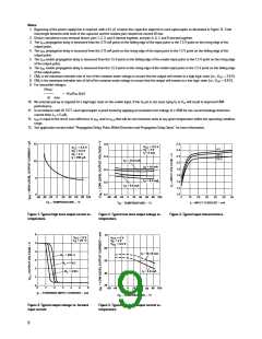
Figure 1. Typical high level output current vs.
temperature.
Figure 2. Typical low level output voltage vs.
temperature.
Figure 3. Typical input characteristics.
6
70
V
T
= 5 V
V
V
V
= 5 V
= 2 V
= 0.6 V
CC
= 25 °C
CC
E
OL
A
5
4
3
2
60
50
I = 10-15 mA
I
R
= 350 Ω
L
R
= 1 KΩ
L
R
= 4 KΩ
I = 5.0 mA
I
L
40
20
1
0
0
1
2
3
4
6
5
-60 -40 -20
0
20 40
80 100
60
I
– FORWARD INPUT CURRENT – mA
F
T
– TEMPERATURE – °C
A
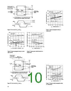
Figure 4. Typical output voltage vs. forward
input current.
Figure 5. Typical low level output current vs.
temperature.
9

 AVAGO [ AVAGO TECHNOLOGIES LIMITED ]