Switching Specifications
Over recommended temperature (TA = 0°C to +70°C), V = 5 V, I = 7.5 mA, unless otherwise specified.
CC
I
Parameter
Symbol
Device
Min.
Typ.* Max. Units
Test Conditions
TA = 25°C
Fig. Note
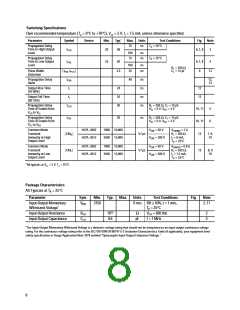
Propagation Delay
Time to High Output
Level
75
ns
tPLH
20
48
6,7, 8
3
100
75
ns
ns
Propagation Delay
Time to Low Output
Level
TA = 25°C
tPHL
25
50
6,7, 8
9
4
100
35
ns
ns
RL = 350 Ω
CL = 15 pF
Pulse Width
Distortion
| tPHL-tPLH
|
3.5
13
Propagation Delay
Skew
tPSK
tr
40
ns
ns
ns
ns
12,
13
Output Rise Time
(10-90%)
24
10
30
12
12
Output Fall Time
(90-10%)
tf
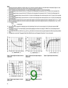
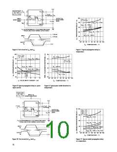
Propagation Delay
Time of Enable from
tELH
RL = 350 Ω, CL = 15 pF,
V = 0 V, VEH = 3 V
EL
10, 11
10, 11
5
6
V
EH to V
EL
Propagation Delay
Time of Enable from
V to V
tEHL
| CMH|
| CML|
20
ns
RL = 350 Ω, CL = 15 pF,
V = 0 V, VEH = 3 V
EL
EL
EH
Common Mode
Transient
Immunity at High
HCPL-2602
HCPL-2612
1000 10,000
3500 15,000
V
CM = 50 V
CM = 300 V
CM = 50 V
CM = 300 V
VO(MIN) = 2 V,
RL = 350 Ω,
II = 0 mA,
V/ µs
V/ µs
13
13
7, 9,
10
V
Output Level
TA = 25°C
Common Mode
Transient
Immunity at Low
HCPL-2602
HCPL-2612
1000 10,000
3500 15,000
V
VO(MAX) = 0.8V,
RL = 350 Ω,
II = 7.5 mA,
TA = 25°C
8, 9
10
V
Output Level
*All typicals at V = 5 V, TA = 25°C.
CC
Package Characteristics
All Typicals at T = 25°C
A
Parameter
Sym.
Min.
Typ. Max. Units
Test Conditions
Fig.
Note
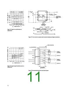
Input-Output Momentary
Withstand Voltage*
V
ISO
3750
V rms RH ≤ 50%, t = 1 min.,
2, 11
T = 25°C
A
Input-Output Resistance
Input-Output Capacitance
R
1012
0.6
Ω
V = 500 Vdc
2
2
I-O
I-O
C
I-O
pF
f = 1 MHz
*The Input-Output Momentary Withstand Voltage is a dielectric voltage rating that should not be interpreted as an input-output continuous voltage
rating. For the continuous voltage rating refer to the IEC/ EN/ DIN EN 60747-5-2 Insulation Characteristics Table (if applicable), your equipment level
safety specification or Avago Application Note 1074 entitled “Optocoupler Input-Output Endurance Voltage.”
8

 AVAGO [ AVAGO TECHNOLOGIES LIMITED ]