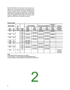
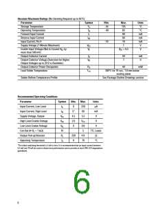
Absolute Maximum Ratings (No Derating Required up to 85°C)
Parameter
Symbol
Min.
-55
Max.
125
85
Units
°C
Storage Temperature
T
S
Operating Temperature
T
A
-40
°C
Forward Input Current
I
60
mA
mA
mA
V
I
Reverse Input Current
I
IR
60
Input Current, Pin 4
-10
10
Supply Voltage (1 Minute Maximum)
V
CC
7
Enable Input Voltage (Not to Exceed V by
V
E
V + 0.5
CC
V
CC
more than 500 mV)
Output Collector Current
I
50
7
mA
V
O
Output Collector Voltage (Selection for Higher
Output Voltages up to 20 V is Available.)
V
O
Output Collector Power Dissipation
Lead Solder Temperature
P
40
mW
O
T
LS
260°C for 10 sec., 1.6 mm below
seating plane
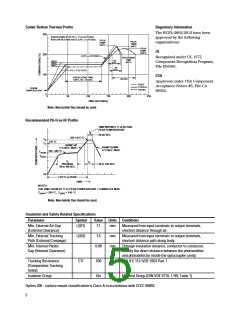
Solder Reflow Temperature Profile
See Package Outline Drawings section
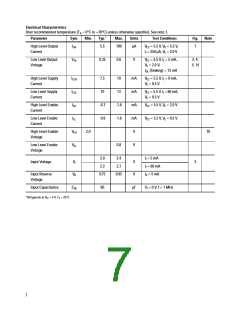
Recommended Operating Conditions
Parameter
Symbol
Min.
0
Max.
250
60
Units
µA
mA
V
Input Current, Low Level
Input Current, High Level
Supply Voltage, Output
High Level Enable Voltage
Low Level Enable Voltage
Fan Out (@ RL = 1 kΩ)
Output Pull-up Resistor
Operating Temperature
I
IL
IIH
5*
4.5
2.0
0
V
CC
5.5
V
EH
V
CC
V
V
EL
0.8
5
V
N
TTL Loads
RL
330
0
4 K
70
Ω
T
A
°C
*The initial switching threshold is 5 mA or less. It is recommended that an input current between
6.3 mA and 10 mA be used to obtain best performance and to provide at least 20% LED degradation
guardband.
6

 AVAGO [ AVAGO TECHNOLOGIES LIMITED ]