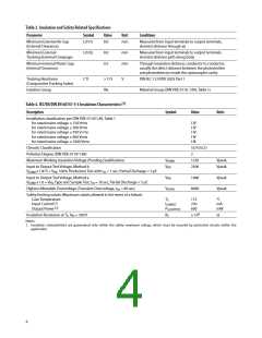
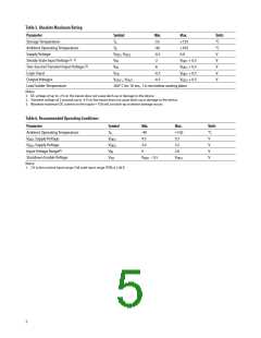
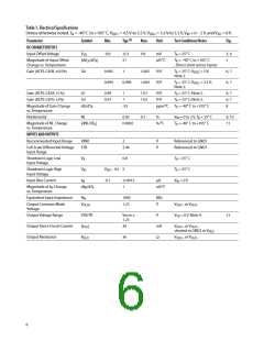
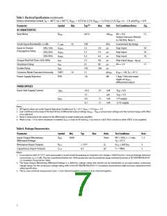
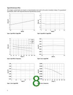
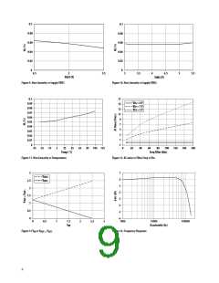
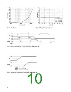
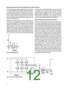
Typical Performance Plots
All ±3(sigma symbol) plots are based on characterization test result at the point of product release0 For guaranteed
specification, refer to the respective Electrical Specifications section0
5
4
3
2
1.5
1
2
0.5
0
1
0
-1
-2
-3
-4
-5
-0.5
-1
-1.5
-2
4.5
5
5.5
3
3.5
4
4.5
5
5.5
Vdd1(V)
Vdd2 (V)
Figure 3. Input Offset vs Supply VDD1
Figure 4. Input Offset vs Supply VDD2
10
8
6
4
2
1.003
1.002
1.001
1.000
0.999
0.998
M+3
Mean
M-3
0
-2
-4
-6
-8
- 10
0.997
4.5
5
Vdd1 (V)
5.5
-55 -35 -15
5
25
45
65
85 105 125
Temp (qC)
Figure 5. Input Offset vs Temperature
Figure 6. Gain vs Supply VDD1
1.00300
1.00200
1.00100
1.00000
0.99900
0.99800
0.99700
1.003
1.002
1.001
1.000
0.999
0.998
0.997
3
3.5
4
4.5
5
5.5
-55 -35 -15
5
25 45 65 85 105 125
Vdd2 (V)
Temp (qC)
Figure 7. Gain vs Supply VDD2
Figure 8. Gain vs Temperature
8

 AVAGO [ AVAGO TECHNOLOGIES LIMITED ]