Table 7. Electrical Specifications
Unless otherwise noted, T = -4±° C to +1±.° C, V
= 40. V to .0. V, V
= 303 V to .0. V, V = ± – 2 V, and V = ± V0
A
DD1
DD2
IN
SD
[1]
Parameter
Symbol
Min.
Typ.
Max.
Unit
Test Conditions/Notes
Fig.
DC CHARACTERISTICS
Input Offset Voltage
VOS
-909
-±03
21
909
mV
TA = 2.° C
3, 4
.
Magnitude of Input Offset
Change vs0 Temperature
|dVOS/dTA|
V/°C
TA = –4±° C to +1±.° C
; Direct short across inputs0
Gain (ACPL-C87B, ±±0.5)
G±
±099.
±0994
1
10±±.
10±±4
V/V
V/V
TA = 2.° C; VDD2 = . V;
Note 20
6, 7
6, 7
±0999
TA = 2.° C; VDD2 = 303 V;
Note 20
Gain (ACPL-C87A, ±15)
Gain (ACPL-C87±, ±35)
G1
±099
±097
1
10±1
10±3
V/V
V/V
TA = 2.° C; Note 20
TA = 2.° C; Note 20
6, 7
6, 7
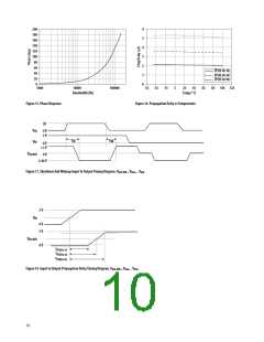
8
G3
1
Magnitude of Gain Change
vs0 Temperature
dG/dTA
-3.
ppm/°C TA = -4±° C to +1±.° C
Nonlinearity
NL
±0±.
±01
5
VIN = ± to 2 V, TA = 2.° C
TA = -4±° C to +1±.° C
9, 1±
11
Magnitude of NL Change
vs0 Temperature
|dNL/dTA|
±0±±±2
5/°C
INPUTS AND OUTPUTS
Recommended Input Range
VINR
FSR
2
V
V
Referenced to GND1
Referenced to GND1
Full-Scale Differential Voltage
Input Range
2046
Shutdown Logic Low
Input Voltage
VIL
±08
.
TA = 2.° C
TA = 2.° C
VIN = ± V
Shutdown Logic ꢀigh
Input Voltage
VIꢀ
VDD – ±0.
-±01
Input Bias Current
IIN
-±0±±1.
1
A
Magnitude of IIN Change
vs0 Temperature
dIIN/dTA
nA/°C
Equivalent Input Impedance
RIN
1±±±
1023
M
Output Common-Mode
Voltage
VOCM
V
VOUT+ or VOUT–
Output Voltage Range
Output Short-Circuit Current
Output Resistance
VOUTR
Vocm ±
1023
V
VSD = ± V0 Note 40
13
|IOSC
|
3±
mA
VOUT+ or VOUT–,
shorted to GND2 or VDD2
ROUT
36
VOUT+ or VOUT–
6

 AVAGO [ AVAGO TECHNOLOGIES LIMITED ]