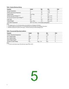
Table 5. Absolute Maximum Rating
Parameter
Symbol
Min.
-..
-4±
-±0.
-2
Max.
Units
°C
°C
V
Storage Temperature
Ambient Operating Temperature
Supply Voltage
Steady-State Input Voltage [1, 3]
Two-Second Transient Input Voltage [2]
Logic Input
TS
+12.
TA
+1±.
VDD1, VDD2
VIN
60±
VDD1 + ±0.
VDD1 + ±0.
VDD1 + ±0.
VDD2 + ±0.
V
VIN
-6
V
VSD
-±0.
-±0.
V
Output Voltages
VOUT+, VOUT−
V
Lead Solder Temperature
Notes:
26±° C for 1± sec0, 106 mm below seating plane
10 DC voltage of up to -2 V on the inputs does not cause latch-up or damage to the device0
20 Transient voltage of 2 seconds up to -6 V on the inputs does not cause latch-up or damage to the device0
30 Absolute maximum DC current on the inputs = 1±± mA, no latch-up or device damage occurs0
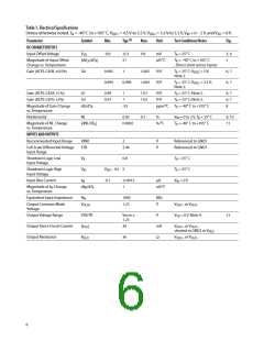
Table 6. Recommended Operating Conditions
Parameter
Symbol
TA
Min.
Max.
+1±.
.0.
Units
°C
V
Ambient Operating Temperature
VDD1 Supply Voltage
VDD2 Supply Voltage
Input Voltage Range[1]
Shutdown Enable Voltage
Notes:
-4±
VDD1
VDD2
VIN
40.
30±
.0.
V
±
20±
V
VSD
VDD1 – ±0.
VDD1
V
10 2 V is the nominal input range0 Full scale input range (FSR) is 2046 V0
.

 AVAGO [ AVAGO TECHNOLOGIES LIMITED ]