Definitions
Gain
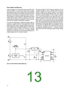
Application Information
Application Circuit
Gain is defined as the slope of the best-fit line of differen- The typical application circuit is shown in Figure 190
tial output voltage (V
range, with offset error adjusted out0
– V
) over the nominal input
The ACPL-C87X voltage sensor is often used in photo-
voltaic (PV) panel voltage measurement and tracking in
PV inverters, and DC bus voltage monitoring in motor
drivers0 The high voltage across rails needs to be scaled
down to fit the input range of the iso-amp by choosing R1
and R2 values according to appropriate ratio0
OUT+
OUT-
Nonlinearity
Nonlinearity is defined as half of the peak-to-peak output
deviation from the best-fit gain line, expressed as a per-
centage of the full-scale differential output voltage0
The ACPL-C87X senses the single-ended input signal
and produces differential outputs across the galvanic
isolation barrier0 The differential outputs (Vout+, Vout-)
can be connected to an op-amp to convert to a single-
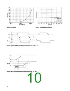
Common Mode Transient Immunity, CMTI, also known
as Common Mode Rejection
CMTI is tested by applying an exponentially rising/falling ended signal or directly to two ADCs0 The op-amp used in
voltage step on pin 4 (GND1) with respect to pin . (GND2)0 the external post-amplifier circuit should be of sufficiently
The rise time of the test waveform is set to approximately high precision so that it does not contribute a significant
.± ns0 The amplitude of the step is adjusted until the dif- amount of offset or offset drift relative to the contribu-
ferential output (V
– V
) exhibits more than a 2±± tion from the isolation amplifier0 Generally, op-amps with
OUT+
OUT-
mV deviation from the average output voltage for more bipolar input stages exhibit better offset performance
than 1μs0 The ACPL-C87x will continue to function if more than op-amps with JFET or MOSFET input stages0
than 1± kV/s common mode slopes are applied, as long
In addition, the op-amp should also have enough
as the breakdown voltage limitations are observed0
bandwidth and slew rate so that it does not adversely
affect the response speed of the overall circuit0 The post-
amplifier circuit includes a pair of capacitors (C4 and C.)
that form a single-pole low-pass filter; these capacitors
allow the bandwidth of the post-amp to be adjusted in-
dependently of the gain and are useful for reducing the
output noise from the isolation amplifier0
Power Supply Rejection, PSR
PSRR is the ratio of differential amplitude of the ripple
outputs over power supply ripple voltage, referred to the
input, expressed in dB0
The gain-setting resistors in the post-amp should have a
tolerance of 15 or better to ensure adequate CMRR and
adequate gain tolerance for the overall circuit0 Resistor
networks can be used that have much better ratio toler-
ances than can be achieved using discrete resistors0 A
resistor network also reduces the total number of compo-
nents for the circuit as well as the required board space0
C5
100 pF
L1
U1
VDD1
VDD1
VDD2
R6
10K, 1%
V+
U2
1
2
3
4
8
7
6
5
VDD2
R1
R3
VIN
VOUT+
10K,1%
Vout
C3
100 nF
R4
10K,1%
ACPL-C87X
SHDN
GND1
VOUT-
R2
10K
C1
C2
OPA237
100 pF 100 nF
GND2
V-
GND1
GND2
R5
10K, 1%
C4
100 pF
L2
GND2
Figure 19. Typical application circuit.
11

 AVAGO [ AVAGO TECHNOLOGIES LIMITED ]