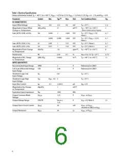
Table 7. Electrical Specifications (continued)
Unless otherwise noted, T = -4±° C to +1±.° C, V
= 40. V to .0. V, V
= 303 V to .0. V, V = ± – 2 V, and V = ± V0
A
DD1
DD2
IN
SD
[1]
Parameter
Symbol
Min.
Typ.
Max. Unit
Test Conditions/Notes
Fig.
AC CHARACTERISTICS
Vout Noise
Nout
±0±13
mVrms Vin = ± V;
12
Output low-pass filtered
to 18± Kꢀz0 Note 30
Small-Signal Bandwidth (-3 dB)
f–3 dB
tPD1±
tPD.±
tPD9±
tR/F
7±
1±±
202
307
.03
207
2.
kꢀz
s
Guaranteed by design
Step input0
Input to Output
.±5-1±5
30±
.0.
60.
40±
4±
18
18
18
Propagation Delay
.±5-.±5
.±5-9±5
s
Step input0
s
Step input0
Output Rise/Fall Time (1±5-9±5)
Shutdown Delay
s
Step input (tPD9± - tPD1±
)
tSD
s
Vin = 2 V
17
Enable Delay
tON
1.±
1.
2±±
s
Common Mode Transient Immunity
Power Supply Rejection
CMTI
PSR
1±
kV/s
dB
VCM = 1 kV, TA = 2.° C
1 Vpp 1 kꢀz sine wave
-78
ripple on VDD1
,
differential output
POWER SUPPLIES
Input Side Supply Current
IDD1
1±0.
1.
1.
mA
A
VSD = ± V
VSD = . V
IDD2
60.
601
12
11
mA
mA
. V supply
303 V supply
Notes:
10 All Typical values are under Typical Operating Conditions at T = 2.° C, V
= . V, V = . V0
DD2
A
DD1
20 Gain is defined as the slope of the best-fit line of differential output voltage (V
error adjusted0
– V
) versus input voltage over the nominal range, with offset
OUT-
OUT+
30 Noise is measured at the output of the differential to single ended post amplifier0
40 When is V = . V or when shutdown is enabled, V
is close to ±V and V
is at close to 2046 V0 This is similar to when VDD1 is not supplied0
SD
out+
out-
Table 8. Package Characteristics
Parameter
Symbol
Min
Typ
Max
Units
Test Conditions
Note
Input-Output Momentary
Withstand Voltage
VISO
.±±±
Vrms
Rꢀ < .±5, t = 1 min0,
TA = 2.° C
1, 2
Resistance (Input-Output)
Capacitance (Input-Output)
Notes:
RI-O
CI-O
> 1±12
±0.
V
I-O = .±± VDC
3
3
pF
f = 1 Mꢀz
10 In accordance with UL 1.77, each optocoupler is proof tested by applying an insulation test voltage ≥ 6±±± Vrms for 1 second (leakage detection
current limit, I ≤ . mA)0 This test is performed before the 1±±5 production test for partial discharge (method b) shown in IEC/EN/DIN EN 6±747-
I-O
.-. Insulation Characteristic Table0
20 The Input-Output Momentary Withstand Voltage is a dielectric voltage rating that should not be interpreted as an input-output continuous
voltage rating0 For the continuous voltage rating, refer to the IEC/EN/DIN EN 6±747-.-. insulation characteristics table and your equipment level
safety specification0
30 This is a two-terminal measurement: pins 1–4 are shorted together and pins .–8 are shorted together0
7

 AVAGO [ AVAGO TECHNOLOGIES LIMITED ]