T5743
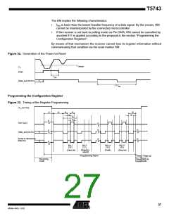
Programming respectively OFF-command is initiated in any case. The registers
OPMODE and LIMIT are set to the default values. RM is cancelled if present.
This period is used if the connected microcontroller detected RM. If the receiver oper-
ates in default mode, this time period for t1 can generally be used.
Note that the capacitive load at Pin DATA is limited.
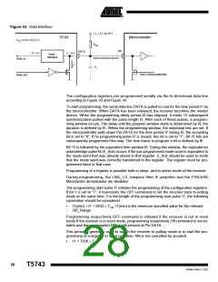
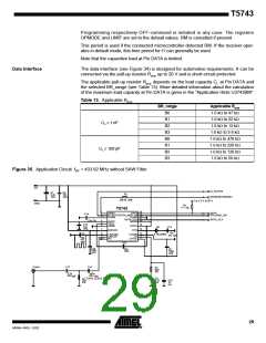
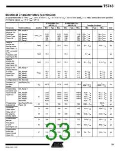
Data Interface
The data interface (see Figure 34) is designed for automotive requirements. It can be
connected via the pull-up resistor Rpup up to 20 V and is short-circuit-protected.
The applicable pull-up resistor Rpup depends on the load capacity CL at Pin DATA and
the selected BR_range (see Table 13). More detailed information about the calculation
of the maximum load capacity at Pin DATA is given in the “Application Hints U3743BM”.
Table 13. Applicable Rpup
BR_range
Applicable Rpup
1.6 kꢃ to 47 kꢃ
1.6 kꢃ to 22 kꢃ
1.6 kꢃ to 12 kꢃ
1.6 kꢃ to 5.6 kꢃ
1.6 kꢃ to 470 kꢃ
1.6 kꢃ to 220 kꢃ
1.6 kꢃ to 120 kꢃ
1.6 kꢃ to 56 kꢃ
B0
B1
B2
B3
B0
B1
B2
B3
CL ? 1 nF
CL ? 100 pF
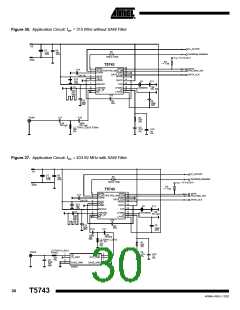
Figure 35. Application Circuit: fRF = 433.92 MHz without SAW Filter
VS
IC_ACTIVE
C7
2.2u
10%
C6
10n
10%
R2
Sensitivity reduction
56k to 150k
V
= 5 V to 20 V
X
GND
R3
>= 1.6k
T5743
1
2
3
20
19
18
17
16
SENS
DATA
DATA
POLLING/_ON
C14
33n 5%
IC_ACTIVE POLLING/_ON
CDEM
DGND
DATA_CLK
MODE
DATA_CLK
4
5
6
AVCC
TEST
AGND
C13
10n
10%
15
14
DVCC
XTO
Q1
C11
12p
7
MIXVCC
8
13
12
11
C3
6.7643MHz
LNAGND
LNA_IN
NC
LFGND
LF
LFVCC
9
2% np0
15p
5%
np0
10
C12
C15
150p
10%
10n
10%
C8
150p
10%
COAX
C17
C16
R1
820
5%
3.3p
5%
100p
5%
np0
np0
L2 TOKO LL2012 F22NJ
C9
4.7n
5%
22n
5%
C10
1n
5%
29
4569A–RKE–12/02

 ATMEL [ ATMEL ]