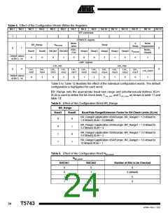
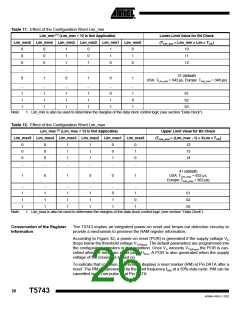
Table 11. Effect of the Configuration Word Lim_min
Lim_min (1) (Lim_min < 10 Is Not Applicable)
Lower Limit Value for Bit Check
Lim_min5 Lim_min4 Lim_min3 Lim_min2 Lim_min1 Lim_min0
(TLim_min = Lim_min × Lim × TClk)
0
0
0
0
1
1
0
0
1
1
0
1
10
11
12
0
0
1
1
0
0
...
...
...
...
...
...
21 (default)
0
1
0
1
0
1
USA: TLim_min = 342 µs, Europe: TLim_min = 348 µs)
...
1
...
1
...
1
...
1
...
0
...
1
61
62
63
1
1
1
1
1
0
1
1
1
1
1
1
Note:
1. Lim_min is also be used to determine the margins of the data clock control logic (see section “Data Clock”).
Table 12. Effect of the Configuration Word Lim_max
Lim_max (1) (Lim_max < 12 Is Not Applicable)
Upper Limit Value for Bit Check
Lim_max5 Lim_max4 Lim_max3 Lim_max2 Lim_max1 Lim_max0
(TLim_max = (Lim_max - 1) × XLim × TClk)
0
0
0
0
1
1
1
1
0
0
0
1
12
13
14
0
0
1
1
1
0
...
...
...
...
...
...
41 (default)
1
0
1
0
0
1
USA: TLim_max = 652 ꢂs,
Europe: TLim_max = 662 µs)
...
1
...
1
...
1
...
1
...
0
...
1
61
62
63
1
1
1
1
1
0
1
1
1
1
1
1
Note:
1. Lim_max is also be used to determine the margins of the data clock control logic (see section “Data Clock”).
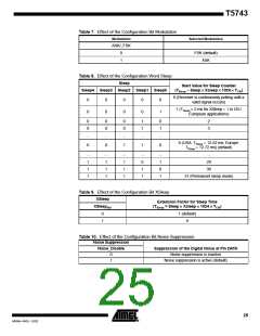
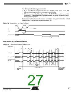
Conservation of the Register
Information
The T5743 implies an integrated power-on reset and brown-out detection circuitry to
provide a mechanism to preserve the RAM register information.
According to Figure 32, a power-on reset (POR) is generated if the supply voltage VS
drops below the threshold voltage VThReset. The default parameters are programmed into
the configuration registers in that condition. Once VS exceeds VThReset the POR is can-
celled after the minimum reset period tRst. A POR is also generated when the supply
voltage of the receiver is turned on.
To indicate that condition, the receiver displays a reset marker (RM) at Pin DATA after a
reset. The RM is represented by the fixed frequency fRM at a 50% duty-cycle. RM can be
cancelled via a Low pulse t1 at Pin DATA.
26
T5743
4569A–RKE–12/02

 ATMEL [ ATMEL ]