T5743
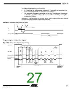
The RM implies the following characteristics:
•
fRM is lower than the lowest feasible frequency of a data signal. By this means, RM
cannot be misinterpreted by the connected microcontroller.
•
If the receiver is set back to polling mode via Pin DATA, RM cannot be cancelled by
accident if t1 is applied according to the proposal in the section “Programming the
Configuration Registers”.
By means of that mechanism the receiver cannot lose its register information without
communicating that condition via the reset marker RM.
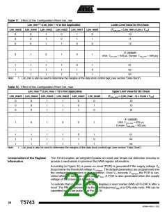
Figure 32. Generation of the Power-on Reset
VThReset
VS
POR
tRst
X
Data_out (DATA)
1 / fRM
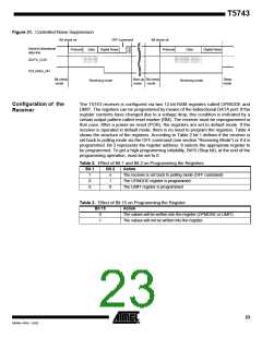
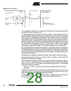
Programming the Configuration Register
Figure 33. Timing of the Register Programming
IC_ACTIVE
t9
t8
t1
t2
t3
t5
t4
t6
t7
Out1 (µC)
Data_out (DATA)
X
X
Serial bi-directional
data line
Bit 1
("0")
(Start bit)
Bit 2
Bit 14
("0")
(Poll8)
Bit 15
("1")
("0")
(Register-
(Stop bit)
select)
T
T
Programming frame
Sleep Start-up
Receiving
mode
Start-up
Sleep
mode
mode
27
4569A–RKE–12/02

 ATMEL [ ATMEL ]