T5743
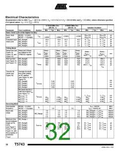
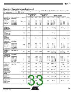
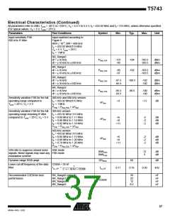
Electrical Characteristics (Continued)
All parameters refer to GND, Tamb = -40LC to +105LC, VS = 4.5 V to 5.5 V, f0 = 433.92 MHz and f0 = 315 MHz, unless otherwise specified.
(For typical values: VS = 5 V, Tamb = 25LC)
6.76438 MHz Osc.
(MODE: 1)
4.90625 MHz Osc.
(MODE: 0)
Variable Oscillator
Min. Typ. Max.
Parameter
Test Conditions
Symbol
Min.
Typ.
Max.
Min.
Typ.
Max.
Unit
Maximum Low BR_Range =
period at Pin
DATA (see
Figure 7 and
Figure 18)
BR_Range0
BR_Range1
BR_Range2
BR_Range3
2152
1076
538
2152
1076
538
2120
1060
530
2120 130 PꢀTXClk
1060 130 PꢀTXClk
130 PꢀTXClk
130 PꢀTXClk
130 PꢀTXClk
130 PꢀTXClk
µs
µs
µs
µs
tDATA_L_max
530
265
130 PꢀTXClk
130 PꢀTXClk
270
270
265
Delay to
activate the
start-up mode
(see Figure 21)
Ton1
Ton2
Ton3
19.7
16.6
17.6
21.8
19.4
16.4
17.4
21.5
9.5 PꢀTClk
10.5 PꢀTClk
µs
µs
µs
OFF- command
at Pin
POLLING/_ON
(see Figure 20)
8 PꢀTClk
Delay to
activate the
sleep mode
(see Figure 20)
19.7
19.4
8.5 PꢀTClk
9.5 PꢀTClk
Pulse on Pin
DATA at the end
of a data
stream (see
Figure 30)
BR_Range =
BR_Range0
BR_Range1
BR_Range2
BR_Range3
16.6
8.3
4.1
2.1
16.6
8.3
4.1
16.3
8.2
4.1
2.0
16.3
8.2
4.1
8 PꢀTClk
4 PꢀTClk
2 PꢀTClk
1 PꢀTClk
8 PꢀTClk
4 PꢀTClk
2 PꢀTClk
1 PꢀTClk
µs
µs
µs
µs
TPulse
2.1
2.0
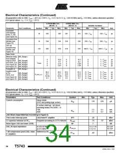
Configuration of the Receiver
Frequency of
the reset
marker
(see Figure 31)
1
1
------------------------------
fRM
117.9
117.9
119.8
119.8
Hz
------------------------------
4096 P T
4096 P T
Clk
Clk
Programming
start pulse (see
Figure 19 and
Figure 33)
BR_Range =
BR_Range0
BR_Range1
BR_Range2
BR_Range3
after POR
3367
2277
1735
1464
16.43
11650
11650
11650
11650
3311
2243
1709
1442
16.18
11470
11470
11470
11470
1624ꢀPꢀTClk
1100PꢀTClk
838 PꢀTClk
707 PꢀTClk
7936 PꢀTClk
5632 PꢀTClk
5632 PꢀTClk
5632 PꢀTClk
5632 PꢀTClk
µs
µs
µs
µs
µs
t1
Programming
delay period
(see Figure 19 and
Figure 33)
385.5 Pꢀ
TClk
t2
t3
795
265
798
265
783
261
786
261
384.5 PꢀTClk
128 PꢀTClk
µs
µs
Synchroni-
zation pulse
128 PꢀTClk
63.5 PꢀTClk
256 PꢀTClk
512 PꢀTClk
Delay until of
the program
window starts
t4
t5
t6
131
530
131
530
129
522
129
522
63.5 PꢀTClk
256 PꢀTClk
512 PꢀTClk
µs
µs
µs
Programming
window
Time frame
of a bit
1060
1060
1044
1044
(see Figure 33)
Programming
pulse (see
Figure 19 and
Figure 33)
t7
132
529
130
521
64 PꢀTClk
256 PꢀTClk
µs
33
4569A–RKE–12/02

 ATMEL [ ATMEL ]