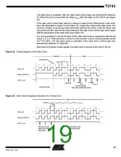
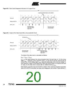
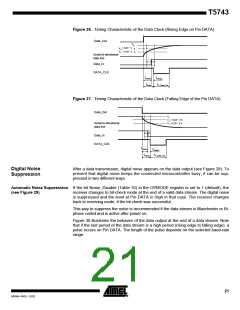
T5743
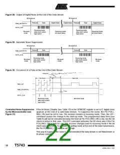
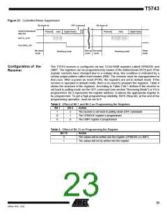
Figure 31. Controlled Noise Suppression
Bit check ok
OFF-command
Digital Noise
Bit check ok
Preburst
Serial bi-directional
data line
Preburst
Data
Data
Digital Noise
(DATA_CLK)
POLLING/_ON
Bit-check
mode
Start-up Bit-check
mode mode
Sleep
mode
Receiving mode
Receiving mode
Configuration of the
Receiver
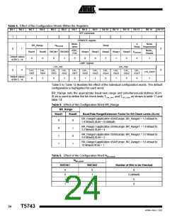
The T5743 receiver is configured via two 12-bit RAM registers called OPMODE and
LIMIT. The registers can be programmed by means of the bidirectional DATA port. If the
register contents have changed due to a voltage drop, this condition is indicated by a
certain output pattern called reset marker (RM). The receiver must be reprogrammed in
that case. After a power-on reset (POR), the registers are set to default mode. If the
receiver is operated in default mode, there is no need to program the registers. Table 4
shows the structure of the registers. According to Table 2 bit 1 defines if the receiver is
set back to polling mode via the OFF-command (see section “Receiving Mode”) or if it is
programmed. Bit 2 represents the register address. It selects the appropriate register to
be programmed. To get a high programming reliability, Bit15 (Stop bit), at the end of the
programming operation, must be set to 0.
Table 2. Effect of Bit 1 and Bit 2 on Programming the Registers
Bit 1
Bit 2
Action
1
0
0
x
1
0
The receiver is set back to polling mode (OFF command)
The OPMODE register is programmed
The LIMIT register is programmed
Table 3. Effect of Bit 15 on Programming the Register
Bit 15
Action
0
1
The values will be written into the register (OPMODE or LIMIT)
The values will not be written into the register
23
4569A–RKE–12/02

 ATMEL [ ATMEL ]