ATmega64A
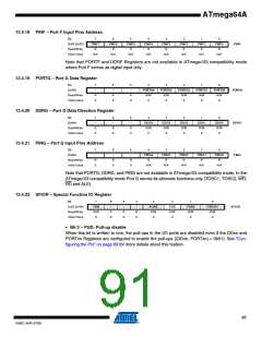
13.4.18 PINF – Port F Input Pins Address
Bit
7
PINF7
R
6
PINF6
R
5
PINF5
R
4
PINF4
R
3
PINF3
R
2
PINF2
R
1
0
0x00 (0x20)
Read/Write
Initial Value
PINF1
R
PINF0
R
PINF
N/A
N/A
N/A
N/A
N/A
N/A
N/A
N/A
Note that PORTF and DDRF Registers are not available in ATmega103 compatibility mode
where Port F serves as digital input only.
13.4.19 PORTG – Port G Data Register
Bit
7
6
–
5
–
4
PORTG4
R/W
0
3
PORTG3
R/W
0
2
PORTG2
R/W
0
1
PORTG1
R/W
0
0
PORTG0
R/W
0
–
R
0
PORTG
DDRG
PING
(0x65)
Read/Write
Initial Value
R
0
R
0
13.4.20 DDRG – Port G Data Direction Register
Bit
7
–
6
–
5
–
4
DDG4
R/W
0
3
DDG3
R/W
0
2
DDG2
R/W
0
1
DDG1
R/W
0
0
DDG0
R/W
0
(0x64)
Read/Write
Initial Value
R
0
R
0
R
0
13.4.21 PING – Port G Input Pins Address
Bit
7
–
6
–
5
–
4
PING4
R
3
PING3
R
2
PING2
R
1
PING1
R
0
PING0
R
(0x63)
Read/Write
Initial Value
R
0
R
0
R
0
N/A
N/A
N/A
N/A
N/A
Note that PORTG, DDRG, and PING are not available in ATmega103 compatibility mode. In the
ATmega103 compatibility mode Port G serves its alternate functions only (TOSC1, TOSC2, WR,
RD and ALE).
13.4.22 SFIOR – Special Function IO Register
Bit
0x20 (0x40)
7
6
5
–
4
–
3
ACME
R/W
0
2
1
PSR0
R/W
0
0
PSR321
R/W
0
TSM
–
PUD
R/W
0
SFIOR
Read/Write
Initial Value
R/W
0
R
0
R
0
R
0
• Bit 2 – PUD: Pull-up disable
When this bit is written to one, the pull-ups in the I/O ports are disabled even if the DDxn and
PORTxn Registers are configured to enable the pull-ups ({DDxn, PORTxn} = 0b01). See “Con-
figuring the Pin” on page 69 for more details about this feature.
91
8160C–AVR–07/09

 ATMEL [ ATMEL ]