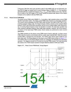
ATmega64A
form generation. Similarly, do not write the TCNT2 value equal to BOTTOM when the counter is
downcounting.
The setup of the OC2 should be performed before setting the Data Direction Register for the port
pin to output. The easiest way of setting the OC2 value is to use the Force Output Compare
(FOC2) strobe bits in Normal mode. The OC2 Register keeps its value even when changing
between Waveform Generation modes.
Be aware that the COM21:0 bits are not double buffered together with the compare value.
Changing the COM21:0 bits will take effect immediately.
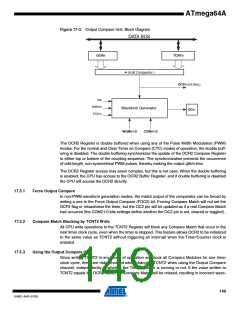
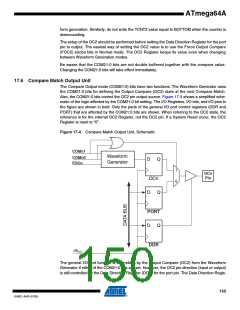
17.6 Compare Match Output Unit
The Compare Output mode (COM21:0) bits have two functions. The Waveform Generator uses
the COM21:0 bits for defining the Output Compare (OC2) state at the next Compare Match.
Also, the COM21:0 bits control the OC2 pin output source. Figure 17-4 shows a simplified sche-
matic of the logic affected by the COM21:0 bit setting. The I/O Registers, I/O bits, and I/O pins in
the figure are shown in bold. Only the parts of the general I/O port control registers (DDR and
PORT) that are affected by the COM21:0 bits are shown. When referring to the OC2 state, the
reference is for the internal OC2 Register, not the OC2 pin. If a System Reset occur, the OC2
Register is reset to “0”.
Figure 17-4. Compare Match Output Unit, Schematic
COMn1
Waveform
Generator
COMn0
FOCn
D
Q
Q
1
0
OCn
Pin
OCn
D
PORT
D
Q
DDR
clkI/O
The general I/O port function is overridden by the Output Compare (OC2) from the Waveform
Generator if either of the COM21:0 bits are set. However, the OC2 pin direction (input or output)
is still controlled by the Data Direction Register (DDR) for the port pin. The Data Direction Regis-
150
8160C–AVR–07/09

 ATMEL [ ATMEL ]