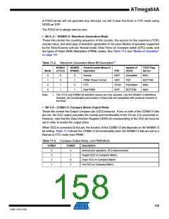
ATmega64A
A frequency (with 50% duty cycle) waveform output in fast PWM mode can be achieved by set-
ting OC2 to toggle its logical level on each Compare Match (COM21:0 = 1). The waveform
generated will have a maximum frequency of fOC2 = fclk_I/O/2 when OCR2 is set to zero. This fea-
ture is similar to the OC2 toggle in CTC mode, except the double buffer feature of the Output
Compare unit is enabled in the fast PWM mode.
17.7.4
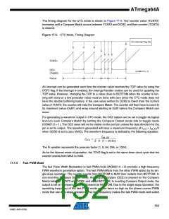
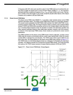
Phase Correct PWM Mode
The phase correct PWM mode (WGM21:0 = 1) provides a high resolution phase correct PWM
waveform generation option. The phase correct PWM mode is based on a dual-slope operation.
The counter counts repeatedly from BOTTOM to MAX and then from MAX to BOTTOM. In non-
inverting Compare Output mode, the Output Compare (OC2) is cleared on the Compare Match
between TCNT2 and OCR2 while upcounting, and set on the Compare Match while downcount-
ing. In inverting Output Compare mode, the operation is inverted. The dual-slope operation has
lower maximum operation frequency than single slope operation. However, due to the symmet-
ric feature of the dual-slope PWM modes, these modes are preferred for motor control
applications.
The PWM resolution for the phase correct PWM mode is fixed to eight bits. In phase correct
PWM mode the counter is incremented until the counter value matches MAX. When the counter
reaches MAX, it changes the count direction. The TCNT2 value will be equal to MAX for one
timer clock cycle. The timing diagram for the phase correct PWM mode is shown on Figure 17-7.
The TCNT2 value is in the timing diagram shown as a histogram for illustrating the dual-slope
operation. The diagram includes non-inverted and inverted PWM outputs. The small horizontal
line marks on the TCNT2 slopes represent Compare Matches between OCR2 and TCNT2.
Figure 17-7. Phase Correct PWM Mode, Timing Diagram
OCn Interrupt
Flag Set
OCRn Update
TOVn Interrupt
Flag Set
TCNTn
(COMn1:0 = 2)
OCn
(COMn1:0 = 3)
OCn
1
2
3
Period
154
8160C–AVR–07/09

 ATMEL [ ATMEL ]