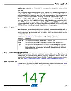
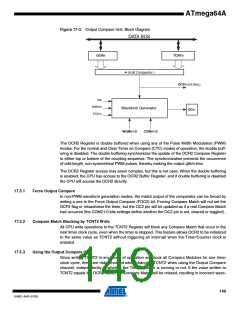
ATmega64A
ter bit for the OC2 pin (DDR_OC2) must be set as output before the OC2 value is visible on the
pin. The port override function is independent of the Waveform Generation mode.
The design of the Output Compare pin logic allows initialization of the OC2 state before the out-
put is enabled. Note that some COM21:0 bit settings are reserved for certain modes of
operation. See “Register Description” on page 157.
17.6.1
Compare Output Mode and Waveform Generation
The Waveform Generator uses the COM21:0 bits differently in Normal, CTC, and PWM modes.
For all modes, setting the COM21:0 = 0 tells the Waveform Generator that no action on the OC2
Register is to be performed on the next Compare Match. For compare output actions in the non-
PWM modes refer to Table 17-3 on page 158. For fast PWM mode, refer to Table 17-4 on page
159, and for phase correct PWM refer to Table 17-5 on page 159.
A change of the COM21:0 bits state will have effect at the first Compare Match after the bits are
written. For non-PWM modes, the action can be forced to have immediate effect by using the
FOC2 strobe bits.
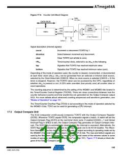
17.7 Modes of Operation
The mode of operation, i.e., the behavior of the Timer/Counter and the Output Compare pins, is
defined by the combination of the Waveform Generation mode (WGM21:0) and Compare Output
mode (COM21:0) bits. The Compare Output mode bits do not affect the counting sequence,
while the Waveform Generation mode bits do. The COM21:0 bits control whether the PWM out-
put generated should be inverted or not (inverted or non-inverted PWM). For non-PWM modes
the COM21:0 bits control whether the output should be set, cleared, or toggled at a Compare
Match (see “Compare Match Output Unit” on page 150).
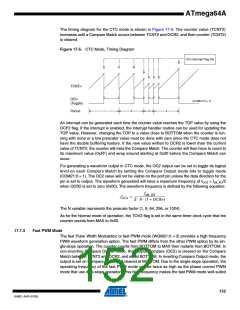
For detailed timing information refer to Figure 17-8, Figure 17-9, Figure 17-10, and Figure 17-11
in “Timer/Counter Timing Diagrams” on page 155.
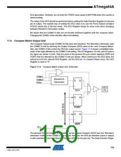
17.7.1
Normal Mode
The simplest mode of operation is the Normal mode (WGM21:0 = 0). In this mode the counting
direction is always up (incrementing), and no counter clear is performed. The counter simply
overruns when it passes its maximum 8-bit value (TOP = 0xFF) and then restarts from the bot-
tom (0x00). In normal operation the Timer/Counter Overflow Flag (TOV2) will be set in the same
timer clock cycle as the TCNT2 becomes zero. The TOV2 flag in this case behaves like a ninth
bit, except that it is only set, not cleared. However, combined with the timer overflow interrupt
that automatically clears the TOV2 flag, the timer resolution can be increased by software. There
are no special cases to consider in the Normal mode, a new counter value can be written
anytime.
The Output Compare unit can be used to generate interrupts at some given time. Using the Out-
put Compare to generate waveforms in Normal mode is not recommended, since this will
occupy too much of the CPU time.
17.7.2
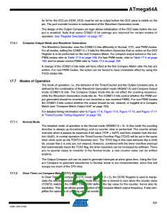
Clear Timer on Compare Match (CTC) Mode
In Clear Timer on Compare or CTC mode (WGM21:0 = 2), the OCR2 Register is used to manip-
ulate the counter resolution. In CTC mode the counter is cleared to zero when the counter value
(TCNT2) matches the OCR2. The OCR2 defines the top value for the counter, hence also its
resolution. This mode allows greater control of the Compare Match output frequency. It also sim-
plifies the operation of counting external events.
151
8160C–AVR–07/09

 ATMEL [ ATMEL ]