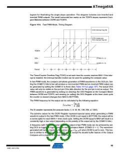
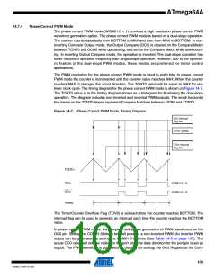
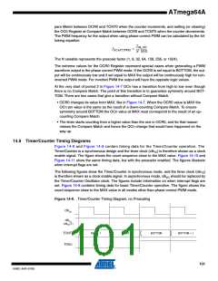
ATmega64A
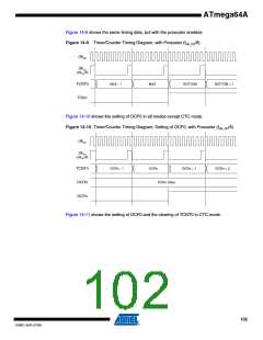
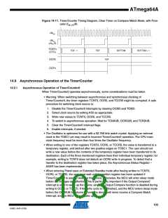
Figure 14-11. Timer/Counter Timing Diagram, Clear Timer on Compare Match Mode, with Pres-
caler (fclk_I/O/8)
clkI/O
clkTn
(clkI/O/8)
TCNTn
(CTC)
TOP - 1
TOP
BOTTOM
BOTTOM + 1
OCRn
TOP
OCFn
14.9 Asynchronous Operation of the Timer/Counter
14.9.1
Asynchronous Operation of Timer/Counter0
When Timer/Counter0 operates asynchronously, some considerations must be taken.
• Warning: When switching between asynchronous and synchronous clocking of
Timer/Counter0, the timer registers TCNT0, OCR0, and TCCR0 might be corrupted. A safe
procedure for switching clock source is:
1. Disable the Timer/Counter0 interrupts by clearing OCIE0 and TOIE0.
2. Select clock source by setting AS0 as appropriate.
3. Write new values to TCNT0, OCR0, and TCCR0.
4. To switch to asynchronous operation: Wait for TCN0UB, OCR0UB, and TCR0UB.
5. Clear the Timer/Counter0 interrupt flags.
6. Enable interrupts, if needed.
• The Oscillator is optimized for use with a 32.768 kHz watch crystal. Applying an external
clock to the TOSC1 pin may result in incorrect Timer/Counter0 operation. The CPU main
clock frequency must be more than four times the Oscillator frequency.
• When writing to one of the registers TCNT0, OCR0, or TCCR0, the value is transferred to a
temporary register, and latched after two positive edges on TOSC1. The user should not
write a new value before the contents of the temporary register have been transferred to its
destination. Each of the three mentioned registers have their individual temporary register, for
example, writing to TCNT0 does not disturb an OCR0 write in progress. To detect that a
transfer to the destination register has taken place, the Asynchronous Status Register –
ASSR has been implemented.
• When entering Power-save or Extended Standby mode after having written to TCNT0,
OCR0, or TCCR0, the user must wait until the written register has been updated if
Timer/Counter0 is used to wake up the device. Otherwise, the MCU will enter sleep mode
before the changes are effective. This is particularly important if the Output Compare0
interrupt is used to wake up the device, since the Output Compare function is disabled during
writing to OCR0 or TCNT0. If the write cycle is not finished, and the MCU enters sleep mode
before the OCR0UB bit returns to zero, the device will never receive a Compare Match
interrupt, and the MCU will not wake up.
103
8160C–AVR–07/09

 ATMEL [ ATMEL ]