ATmega48/88/168
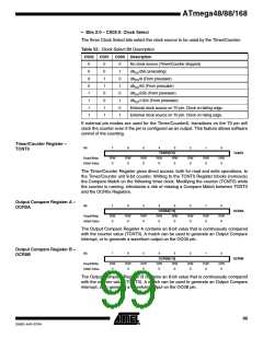
• Bits 2:0 – CS02:0: Clock Select
The three Clock Select bits select the clock source to be used by the Timer/Counter.
Table 52. Clock Select Bit Description
CS02
CS01
CS00 Description
0
0
0
0
1
1
1
1
0
0
1
1
0
0
1
1
0
1
0
1
0
1
0
1
No clock source (Timer/Counter stopped)
clkI/O/(No prescaling)
clkI/O/8 (From prescaler)
clkI/O/64 (From prescaler)
clkI/O/256 (From prescaler)
clkI/O/1024 (From prescaler)
External clock source on T0 pin. Clock on falling edge.
External clock source on T0 pin. Clock on rising edge.
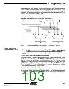
If external pin modes are used for the Timer/Counter0, transitions on the T0 pin will
clock the counter even if the pin is configured as an output. This feature allows software
control of the counting.
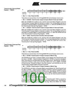
Timer/Counter Register –
TCNT0
Bit
7
6
5
4
3
2
1
0
TCNT0[7:0]
TCNT0
Read/Write
Initial Value
R/W
0
R/W
0
R/W
0
R/W
0
R/W
0
R/W
0
R/W
0
R/W
0
The Timer/Counter Register gives direct access, both for read and write operations, to
the Timer/Counter unit 8-bit counter. Writing to the TCNT0 Register blocks (removes)
the Compare Match on the following timer clock. Modifying the counter (TCNT0) while
the counter is running, introduces a risk of missing a Compare Match between TCNT0
and the OCR0x Registers.
Output Compare Register A –
OCR0A
Bit
7
6
5
4
3
2
1
0
OCR0A[7:0]
R/W R/W
OCR0A
Read/Write
Initial Value
R/W
0
R/W
0
R/W
0
R/W
0
R/W
0
R/W
0
0
0
The Output Compare Register A contains an 8-bit value that is continuously compared
with the counter value (TCNT0). A match can be used to generate an Output Compare
interrupt, or to generate a waveform output on the OC0A pin.
Output Compare Register B –
OCR0B
Bit
7
6
5
4
3
2
1
0
OCR0B[7:0]
R/W R/W
OCR0B
Read/Write
Initial Value
R/W
0
R/W
0
R/W
0
R/W
0
R/W
0
R/W
0
0
0
The Output Compare Register B contains an 8-bit value that is continuously compared
with the counter value (TCNT0). A match can be used to generate an Output Compare
interrupt, or to generate a waveform output on the OC0B pin.
99
2545D–AVR–07/04

 ATMEL [ ATMEL ]