ATmega48/88/168
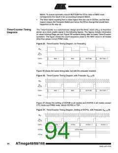
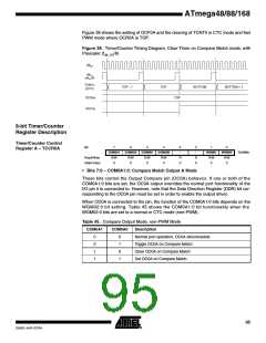
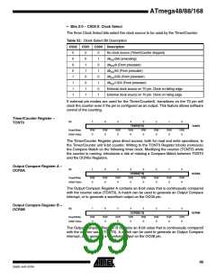
Figure 38 shows the setting of OCF0A and the clearing of TCNT0 in CTC mode and fast
PWM mode where OCR0A is TOP.
Figure 38. Timer/Counter Timing Diagram, Clear Timer on Compare Match mode, with
Prescaler (fclk_I/O/8)
clkI/O
clkTn
(clkI/O/8)
TCNTn
(CTC)
TOP - 1
TOP
BOTTOM
BOTTOM + 1
OCRnx
TOP
OCFnx
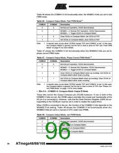
8-bit Timer/Counter
Register Description
Timer/Counter Control
Register A – TCCR0A
Bit
7
COM0A1
R/W
6
COM0A0
5
COM0B1
R/W
4
COM0B0
R/W
3
2
–
1
WGM01
R/W
0
0
WGM00
–
R
0
TCCR0A
Read/Write
Initial Value
R/W
0
R
0
R/W
0
0
0
0
• Bits 7:6 – COM0A1:0: Compare Match Output A Mode
These bits control the Output Compare pin (OC0A) behavior. If one or both of the
COM0A1:0 bits are set, the OC0A output overrides the normal port functionality of the
I/O pin it is connected to. However, note that the Data Direction Register (DDR) bit cor-
responding to the OC0A pin must be set in order to enable the output driver.
When OC0A is connected to the pin, the function of the COM0A1:0 bits depends on the
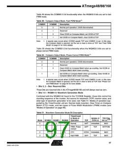
WGM02:0 bit setting. Table 45 shows the COM0A1:0 bit functionality when the
WGM02:0 bits are set to a normal or CTC mode (non-PWM).
Table 45. Compare Output Mode, non-PWM Mode
COM0A1
COM0A0
Description
0
0
1
1
0
1
0
1
Normal port operation, OC0A disconnected.
Toggle OC0A on Compare Match
Clear OC0A on Compare Match
Set OC0A on Compare Match
95
2545D–AVR–07/04

 ATMEL [ ATMEL ]