ATmega48/88/168
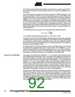
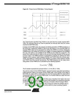
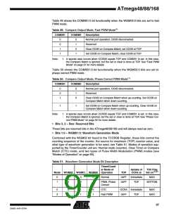
Figure 34. Phase Correct PWM Mode, Timing Diagram
OCnx Interrupt Flag Set
OCRnx Update
TOVn Interrupt Flag Set
TCNTn
(COMnx1:0 = 2)
(COMnx1:0 = 3)
OCnx
OCnx
1
2
3
Period
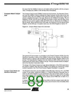
The Timer/Counter Overflow Flag (TOV0) is set each time the counter reaches BOT-
TOM. The Interrupt Flag can be used to generate an interrupt each time the counter
reaches the BOTTOM value.
In phase correct PWM mode, the compare unit allows generation of PWM waveforms on
the OC0x pins. Setting the COM0x1:0 bits to two will produce a non-inverted PWM. An
inverted PWM output can be generated by setting the COM0x1:0 to three: Setting the
COM0A0 bits to one allows the OC0A pin to toggle on Compare Matches if the WGM02
bit is set. This option is not available for the OC0B pin (see Table 50 on page 97). The
actual OC0x value will only be visible on the port pin if the data direction for the port pin
is set as output. The PWM waveform is generated by clearing (or setting) the OC0x
Register at the compare match between OCR0x and TCNT0 when the counter incre-
ments, and setting (or clearing) the OC0x Register at compare match between OCR0x
and TCNT0 when the counter decrements. The PWM frequency for the output when
using phase correct PWM can be calculated by the following equation:
f
clk_I/O
f
= -----------------
OCnxPCPWM
N ⋅ 510
The N variable represents the prescale factor (1, 8, 64, 256, or 1024).
The extreme values for the OCR0A Register represent special cases when generating a
PWM waveform output in the phase correct PWM mode. If the OCR0A is set equal to
BOTTOM, the output will be continuously low and if set equal to MAX the output will be
continuously high for non-inverted PWM mode. For inverted PWM the output will have
the opposite logic values.
At the very start of period 2 in Figure 34 OCnx has a transition from high to low even
though there is no Compare Match. The point of this transition is to guarantee symmetry
around BOTTOM. There are two cases that give a transition without Compare Match.
•
OCRnx changes its value from MAX, like in Figure 34. When the OCR0A value is
MAX the OCn pin value is the same as the result of a down-counting Compare
93
2545D–AVR–07/04

 ATMEL [ ATMEL ]