ATmega48/88/168
nected between the AIO outputs shown in the port figure and the digital logic of the
TWI module.
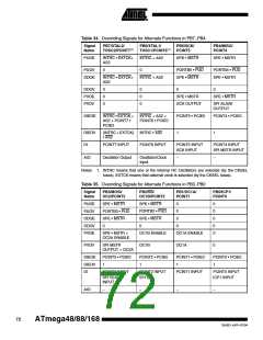
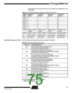
Table 38. Overriding Signals for Alternate Functions in PC3..PC0
Signal PC3/ADC3/
PC2/ADC2/
PCINT10
PC1/ADC1/
PCINT9
PC0/ADC0/
PCINT8
Name
PUOE
PUOV
DDOE
DDOV
PVOE
PVOV
PCINT11
0
0
0
0
0
0
0
0
0
0
0
0
0
0
0
0
0
0
0
0
0
0
0
0
DIEOE PCINT11 • PCIE1
+ ADC3D
PCINT10 • PCIE1
+ ADC2D
PCINT9 • PCIE1 +
ADC1D
PCINT8 • PCIE1 +
ADC0D
DIEOV PCINT11 • PCIE1
PCINT10 • PCIE1
PCINT10 INPUT
ADC2 INPUT
PCINT9 • PCIE1
PCINT9 INPUT
ADC1 INPUT
PCINT8 • PCIE1
PCINT8 INPUT
ADC0 INPUT
DI
PCINT11 INPUT
ADC3 INPUT
AIO
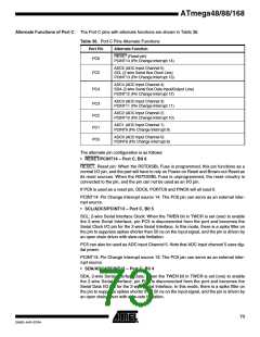
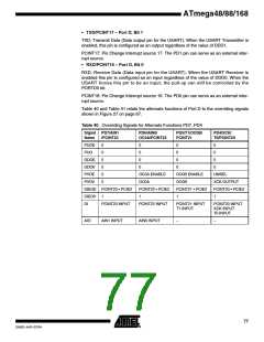
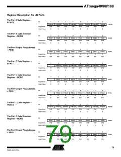
Alternate Functions of Port D The Port D pins with alternate functions are shown in Table 39.
Table 39. Port D Pins Alternate Functions
Port Pin
Alternate Function
AIN1 (Analog Comparator Negative Input)
PCINT23 (Pin Change Interrupt 23)
PD7
AIN0 (Analog Comparator Positive Input)
PD6
PD5
PD4
PD3
OC0A (Timer/Counter0 Output Compare Match A Output)
PCINT22 (Pin Change Interrupt 22)
T1 (Timer/Counter 1 External Counter Input)
OC0B (Timer/Counter0 Output Compare Match B Output)
PCINT21 (Pin Change Interrupt 21)
XCK (USART External Clock Input/Output)
T0 (Timer/Counter 0 External Counter Input)
PCINT20 (Pin Change Interrupt 20)
INT1 (External Interrupt 1 Input)
OC2B (Timer/Counter2 Output Compare Match B Output)
PCINT19 (Pin Change Interrupt 19)
INT0 (External Interrupt 0 Input)
PCINT18 (Pin Change Interrupt 18)
PD2
PD1
PD0
TXD (USART Output Pin)
PCINT17 (Pin Change Interrupt 17)
RXD (USART Input Pin)
PCINT16 (Pin Change Interrupt 16)
The alternate pin configuration is as follows:
• AIN1/OC2B/PCINT23 – Port D, Bit 7
75
2545D–AVR–07/04

 ATMEL [ ATMEL ]