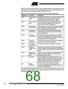
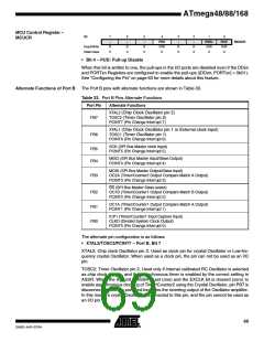
ATmega48/88/168
driven low. When the SPI is enabled as a Master, the data direction of this pin is con-
trolled by DDB2. When the pin is forced by the SPI to be an input, the pull-up can still be
controlled by the PORTB2 bit.
OC1B, Output Compare Match output: The PB2 pin can serve as an external output for
the Timer/Counter1 Compare Match B. The PB2 pin has to be configured as an output
(DDB2 set (one)) to serve this function. The OC1B pin is also the output pin for the PWM
mode timer function.
PCINT2: Pin Change Interrupt source 2. The PB2 pin can serve as an external interrupt
source.
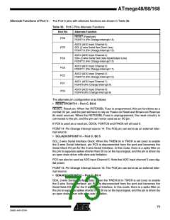
• OC1A/PCINT1 – Port B, Bit 1
OC1A, Output Compare Match output: The PB1 pin can serve as an external output for
the Timer/Counter1 Compare Match A. The PB1 pin has to be configured as an output
(DDB1 set (one)) to serve this function. The OC1A pin is also the output pin for the PWM
mode timer function.
PCINT1: Pin Change Interrupt source 1. The PB1 pin can serve as an external interrupt
source.
• ICP1/CLKO/PCINT0 – Port B, Bit 0
ICP1, Input Capture Pin: The PB0 pin can act as an Input Capture Pin for
Timer/Counter1.
CLKO, Divided System Clock: The divided system clock can be output on the PB0 pin.
The divided system clock will be output if the CKOUT Fuse is programmed, regardless
of the PORTB0 and DDB0 settings. It will also be output during reset.
PCINT0: Pin Change Interrupt source 0. The PB0 pin can serve as an external interrupt
source.
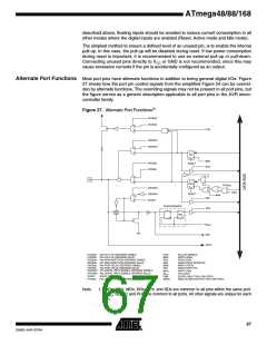
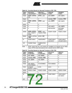
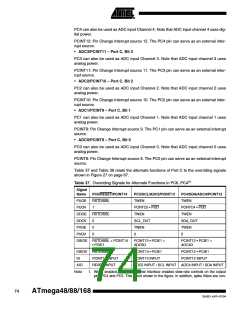
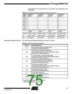
Table 34 and Table 35 relate the alternate functions of Port B to the overriding signals
shown in Figure 27 on page 67. SPI MSTR INPUT and SPI SLAVE OUTPUT constitute
the MISO signal, while MOSI is divided into SPI MSTR OUTPUT and SPI SLAVE
INPUT.
71
2545D–AVR–07/04

 ATMEL [ ATMEL ]