PC4 can also be used as ADC input Channel 4. Note that ADC input channel 4 uses dig-
ital power.
PCINT12: Pin Change Interrupt source 12. The PC4 pin can serve as an external inter-
rupt source.
• ADC3/PCINT11 – Port C, Bit 3
PC3 can also be used as ADC input Channel 3. Note that ADC input channel 3 uses
analog power.
PCINT11: Pin Change Interrupt source 11. The PC3 pin can serve as an external inter-
rupt source.
• ADC2/PCINT10 – Port C, Bit 2
PC2 can also be used as ADC input Channel 2. Note that ADC input channel 2 uses
analog power.
PCINT10: Pin Change Interrupt source 10. The PC2 pin can serve as an external inter-
rupt source.
• ADC1/PCINT9 – Port C, Bit 1
PC1 can also be used as ADC input Channel 1. Note that ADC input channel 1 uses
analog power.
PCINT9: Pin Change Interrupt source 9. The PC1 pin can serve as an external interrupt
source.
• ADC0/PCINT8 – Port C, Bit 0
PC0 can also be used as ADC input Channel 0. Note that ADC input channel 0 uses
analog power.
PCINT8: Pin Change Interrupt source 8. The PC0 pin can serve as an external interrupt
source.
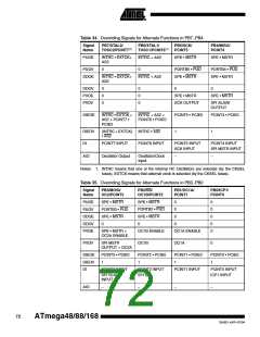
Table 37 and Table 38 relate the alternate functions of Port C to the overriding signals
shown in Figure 27 on page 67.
Table 37. Overriding Signals for Alternate Functions in PC6..PC4(1)
Signal
Name
PUOE
PUOV
DDOE
DDOV
PVOE
PVOV
PC6/RESET/PCINT14
PC5/SCL/ADC5/PCINT13
PC4/SDA/ADC4/PCINT12
RSTDISBL
TWEN
TWEN
1
PORTC5 • PUD
TWEN
PORTC4 • PUD
TWEN
RSTDISBL
0
0
0
SCL_OUT
TWEN
SDA_OUT
TWEN
0
0
DIEOE RSTDISBL + PCINT14
• PCIE1
PCINT13 • PCIE1 +
ADC5D
PCINT12 • PCIE1 +
ADC4D
DIEOV RSTDISBL
PCINT13 • PCIE1
PCINT13 INPUT
PCINT12 • PCIE1
PCINT12 INPUT
DI
PCINT14 INPUT
RESET INPUT
AIO
ADC5 INPUT / SCL INPUT ADC4 INPUT / SDA INPUT
Note:
1. When enabled, the 2-wire Serial Interface enables slew-rate controls on the output
pins PC4 and PC5. This is not shown in the figure. In addition, spike filters are con-
74
ATmega48/88/168
2545D–AVR–07/04

 ATMEL [ ATMEL ]