ATmega48/88/168
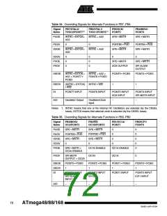
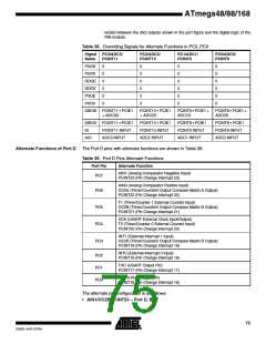
Alternate Functions of Port C The Port C pins with alternate functions are shown in Table 36.
Table 36. Port C Pins Alternate Functions
Port Pin
Alternate Function
RESET (Reset pin)
PCINT14 (Pin Change Interrupt 14)
PC6
ADC5 (ADC Input Channel 5)
PC5
PC4
SCL (2-wire Serial Bus Clock Line)
PCINT13 (Pin Change Interrupt 13)
ADC4 (ADC Input Channel 4)
SDA (2-wire Serial Bus Data Input/Output Line)
PCINT12 (Pin Change Interrupt 12)
ADC3 (ADC Input Channel 3)
PCINT11 (Pin Change Interrupt 11)
PC3
PC2
PC1
PC0
ADC2 (ADC Input Channel 2)
PCINT10 (Pin Change Interrupt 10)
ADC1 (ADC Input Channel 1)
PCINT9 (Pin Change Interrupt 9)
ADC0 (ADC Input Channel 0)
PCINT8 (Pin Change Interrupt 8)
The alternate pin configuration is as follows:
• RESET/PCINT14 – Port C, Bit 6
RESET, Reset pin: When the RSTDISBL Fuse is programmed, this pin functions as a
normal I/O pin, and the part will have to rely on Power-on Reset and Brown-out Reset as
its reset sources. When the RSTDISBL Fuse is unprogrammed, the reset circuitry is
connected to the pin, and the pin can not be used as an I/O pin.
If PC6 is used as a reset pin, DDC6, PORTC6 and PINC6 will all read 0.
PCINT14: Pin Change Interrupt source 14. The PC6 pin can serve as an external inter-
rupt source.
• SCL/ADC5/PCINT13 – Port C, Bit 5
SCL, 2-wire Serial Interface Clock: When the TWEN bit in TWCR is set (one) to enable
the 2-wire Serial Interface, pin PC5 is disconnected from the port and becomes the
Serial Clock I/O pin for the 2-wire Serial Interface. In this mode, there is a spike filter on
the pin to suppress spikes shorter than 50 ns on the input signal, and the pin is driven by
an open drain driver with slew-rate limitation.
PC5 can also be used as ADC input Channel 5. Note that ADC input channel 5 uses dig-
ital power.
PCINT13: Pin Change Interrupt source 13. The PC5 pin can serve as an external inter-
rupt source.
• SDA/ADC4/PCINT12 – Port C, Bit 4
SDA, 2-wire Serial Interface Data: When the TWEN bit in TWCR is set (one) to enable
the 2-wire Serial Interface, pin PC4 is disconnected from the port and becomes the
Serial Data I/O pin for the 2-wire Serial Interface. In this mode, there is a spike filter on
the pin to suppress spikes shorter than 50 ns on the input signal, and the pin is driven by
an open drain driver with slew-rate limitation.
73
2545D–AVR–07/04

 ATMEL [ ATMEL ]