PCINT7: Pin Change Interrupt source 7. The PB7 pin can serve as an external interrupt
source.
If PB7 is used as a clock pin, DDB7, PORTB7 and PINB7 will all read 0.
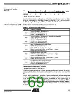
• XTAL1/TOSC1/PCINT6 – Port B, Bit 6
XTAL1: Chip clock Oscillator pin 1. Used for all chip clock sources except internal cali-
brated RC Oscillator. When used as a clock pin, the pin can not be used as an I/O pin.
TOSC1: Timer Oscillator pin 1. Used only if internal calibrated RC Oscillator is selected
as chip clock source, and the asynchronous timer is enabled by the correct setting in
ASSR. When the AS2 bit in ASSR is set (one) to enable asynchronous clocking of
Timer/Counter2, pin PB6 is disconnected from the port, and becomes the input of the
inverting Oscillator amplifier. In this mode, a crystal Oscillator is connected to this pin,
and the pin can not be used as an I/O pin.
PCINT6: Pin Change Interrupt source 6. The PB6 pin can serve as an external interrupt
source.
If PB6 is used as a clock pin, DDB6, PORTB6 and PINB6 will all read 0.
• SCK/PCINT5 – Port B, Bit 5
SCK: Master Clock output, Slave Clock input pin for SPI channel. When the SPI is
enabled as a Slave, this pin is configured as an input regardless of the setting of DDB5.
When the SPI is enabled as a Master, the data direction of this pin is controlled by
DDB5. When the pin is forced by the SPI to be an input, the pull-up can still be con-
trolled by the PORTB5 bit.
PCINT5: Pin Change Interrupt source 5. The PB5 pin can serve as an external interrupt
source.
• MISO/PCINT4 – Port B, Bit 4
MISO: Master Data input, Slave Data output pin for SPI channel. When the SPI is
enabled as a Master, this pin is configured as an input regardless of the setting of
DDB4. When the SPI is enabled as a Slave, the data direction of this pin is controlled by
DDB4. When the pin is forced by the SPI to be an input, the pull-up can still be con-
trolled by the PORTB4 bit.
PCINT4: Pin Change Interrupt source 4. The PB4 pin can serve as an external interrupt
source.
• MOSI/OC2/PCINT3 – Port B, Bit 3
MOSI: SPI Master Data output, Slave Data input for SPI channel. When the SPI is
enabled as a Slave, this pin is configured as an input regardless of the setting of DDB3.
When the SPI is enabled as a Master, the data direction of this pin is controlled by
DDB3. When the pin is forced by the SPI to be an input, the pull-up can still be con-
trolled by the PORTB3 bit.
OC2, Output Compare Match Output: The PB3 pin can serve as an external output for
the Timer/Counter2 Compare Match. The PB3 pin has to be configured as an output
(DDB3 set (one)) to serve this function. The OC2 pin is also the output pin for the PWM
mode timer function.
PCINT3: Pin Change Interrupt source 3. The PB3 pin can serve as an external interrupt
source.
• SS/OC1B/PCINT2 – Port B, Bit 2
SS: Slave Select input. When the SPI is enabled as a Slave, this pin is configured as an
input regardless of the setting of DDB2. As a Slave, the SPI is activated when this pin is
70
ATmega48/88/168
2545D–AVR–07/04

 ATMEL [ ATMEL ]