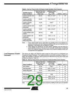
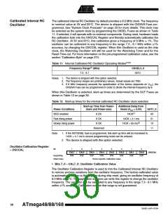
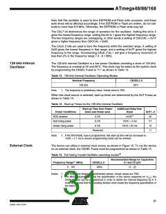
ATmega48/88/168
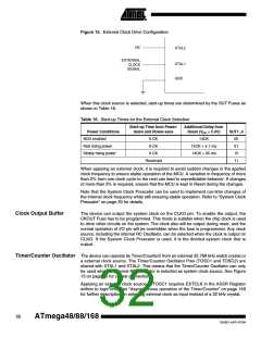
System Clock Prescaler
The ATmega48/88/168 has a system clock prescaler, and the system clock can be
divided by setting the “Clock Prescale Register – CLKPR” on page 337. This feature can
be used to decrease the system clock frequency and the power consumption when the
requirement for processing power is low. This can be used with all clock source options,
and it will affect the clock frequency of the CPU and all synchronous peripherals. clkI/O,
clkADC, clkCPU, and clkFLASH are divided by a factor as shown in Table 20 on page 41.
When switching between prescaler settings, the System Clock Prescaler ensures that
no glitches occurs in the clock system. It also ensures that no intermediate frequency is
higher than neither the clock frequency corresponding to the previous setting, nor the
clock frequency corresponding to the new setting. The ripple counter that implements
the prescaler runs at the frequency of the undivided clock, which may be faster than the
CPU's clock frequency. Hence, it is not possible to determine the state of the prescaler -
even if it were readable, and the exact time it takes to switch from one clock division to
the other cannot be exactly predicted. From the time the CLKPS values are written, it
takes between T1 + T2 and T1 + 2 * T2 before the new clock frequency is active. In this
interval, 2 active clock edges are produced. Here, T1 is the previous clock period, and
T2 is the period corresponding to the new prescaler setting.
To avoid unintentional changes of clock frequency, a special write procedure must
befollowed to change the CLKPS bits:
1. Write the Clock Prescaler Change Enable (CLKPCE) bit to one and all other
bitsin CLKPR to zero.
2. Within four cycles, write the desired value to CLKPS while writing a zero to
CLKPCE.
Interrupts must be disabled when changing prescaler setting to make sure the write pro-
cedure is not interrupted.
Clock Prescale Register –
CLKPR
Bit
7
CLKPCE
R/W
0
6
–
5
–
4
–
3
2
1
0
CLKPS3
R/W
CLKPS2
R/W
CLKPS1
R/W
CLKPS0
R/W
CLKPR
Read/Write
Initial Value
R
0
R
0
R
0
See Bit Description
• Bit 7 – CLKPCE: Clock Prescaler Change Enable
The CLKPCE bit must be written to logic one to enable change of the CLKPS bits. The
CLKPCE bit is only updated when the other bits in CLKPR are simultaneously written to
zero. CLKPCE is cleared by hardware four cycles after it is written or when CLKPS bits
are written. Rewriting the CLKPCE bit within this time-out period does neither extend the
time-out period, nor clear the CLKPCE bit.
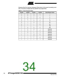
• Bits 3..0 – CLKPS3..0: Clock Prescaler Select Bits 3 - 0
These bits define the division factor between the selected clock source and the internal
system clock. These bits can be written run-time to vary the clock frequency to suit the
application requirements. As the divider divides the master clock input to the MCU, the
speed of all synchronous peripherals is reduced when a division factor is used. The divi-
sion factors are given in Table 17.
The CKDIV8 Fuse determines the initial value of the CLKPS bits. If CKDIV8 is unpro-
grammed, the CLKPS bits will be reset to “0000”. If CKDIV8 is programmed, CLKPS bits
are reset to “0011”, giving a division factor of 8 at start up. This feature should be used if
the selected clock source has a higher frequency than the maximum frequency of the
device at the present operating conditions. Note that any value can be written to the
CLKPS bits regardless of the CKDIV8 Fuse setting. The Application software must
ensure that a sufficient division factor is chosen if the selected clock source has a higher
33
2545D–AVR–07/04

 ATMEL [ ATMEL ]