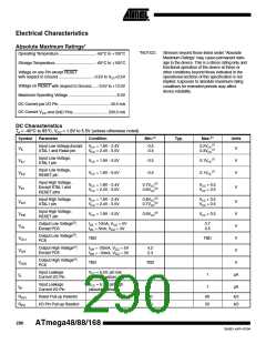
5. All DC Characteristics contained in this datasheet are based on simulation and characterization of other AVR microcontrol-
lers manufactured in the same process technology. These values are preliminary values representing design targets, and
will be updated after characterization of actual silicon
6. Values with “Power Reduction Register - PRR” disabled (0x00).
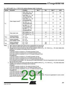
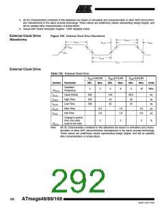
External Clock Drive
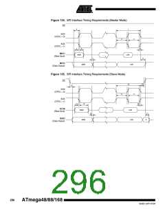
Figure 130. External Clock Drive Waveforms
Waveforms
V
IH1
V
IL1
External Clock Drive
Table 132. External Clock Drive
VCC=1.8-5.5V
VCC=2.7-5.5V
VCC=4.5-5.5V
Symbol Parameter
Min.
Max.
Min.
Max.
Min.
Max.
Units
Oscillator
0
2
0
8
0
16
MHz
1/tCLCL
tCLCL
Frequency
Clock Period
High Time
Low Time
Rise Time
Fall Time
500
200
200
125
50
62.5
25
ns
ns
ns
µs
µs
tCHCX
tCLCX
tCLCH
tCHCL
50
25
2.0
2.0
1.6
1.6
0.5
0.5
Change in period
from one clock
cycle to the next
2
2
2
ꢀ
∆tCLCL
Note:
All DC Characteristics contained in this datasheet are based on simulation and charac-
terization of other AVR microcontrollers manufactured in the same process technology.
These values are preliminary values representing design targets, and will be updated
after characterization of actual silicon.
292
ATmega48/88/168
2545D–AVR–07/04

 ATMEL [ ATMEL ]