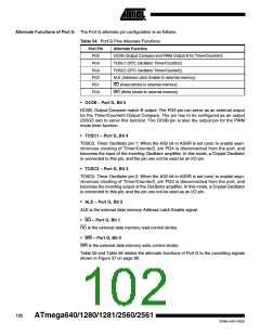
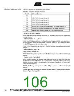
Alternate Functions of Port G The Port G alternate pin configuration is as follows:
Table 54. Port G Pins Alternate Functions
Port Pin
PG5
Alternate Function
OC0B (Output Compare and PWM Output B for Timer/Counter0)
TOSC1 (RTC Oscillator Timer/Counter2)
TOSC2 (RTC Oscillator Timer/Counter2)
ALE (Address Latch Enable to external memory)
RD (Read strobe to external memory)
WR (Write strobe to external memory)
PG4
PG3
PG2
PG1
PG0
• OC0B – Port G, Bit 5
OC0B, Output Compare match B output: The PG5 pin can serve as an external output
for the TImer/Counter0 Output Compare. The pin has to be configured as an output
(DDG5 set) to serve this function. The OC0B pin is also the output pin for the PWM
mode timer function.
• TOSC1 – Port G, Bit 4
TOSC2, Timer Oscillator pin 1: When the AS2 bit in ASSR is set (one) to enable asyn-
chronous clocking of Timer/Counter2, pin PG4 is disconnected from the port, and
becomes the input of the inverting Oscillator amplifier. In this mode, a Crystal Oscillator
is connected to this pin, and the pin can not be used as an I/O pin.
• TOSC2 – Port G, Bit 3
TOSC2, Timer Oscillator pin 2: When the AS2 bit in ASSR is set (one) to enable asyn-
chronous clocking of Timer/Counter2, pin PG3 is disconnected from the port, and
becomes the inverting output of the Oscillator amplifier. In this mode, a Crystal Oscillator
is connected to this pin, and the pin can not be used as an I/O pin.
• ALE – Port G, Bit 2
ALE is the external data memory Address Latch Enable signal.
• RD – Port G, Bit 1
RD is the external data memory read control strobe.
• WR – Port G, Bit 0
WR is the external data memory write control strobe.
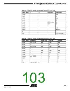
Table 55 and Table 56 relates the alternate functions of Port G to the overriding signals
shown in Figure 37 on page 86.
102
ATmega640/1280/1281/2560/2561
2549A–AVR–03/05

 ATMEL [ ATMEL ]