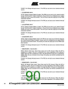
The simplest method to ensure a defined level of an unused pin, is to enable the internal
pull-up. In this case, the pull-up will be disabled during reset. If low power consumption
during reset is important, it is recommended to use an external pull-up or pull-down.
Connecting unused pins directly to VCC or GND is not recommended, since this may
cause excessive currents if the pin is accidentally configured as an output.
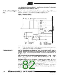
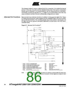
Alternate Port Functions Most port pins have alternate functions in addition to being general digital I/Os. Figure
37 shows how the port pin control signals from the simplified Figure 34 can be overrid-
den by alternate functions. The overriding signals may not be present in all port pins, but
the figure serves as a generic description applicable to all port pins in the AVR micro-
controller family.
Figure 37. Alternate Port Functions(1)
PUOExn
PUOVxn
1
PUD
0
DDOExn
DDOVxn
1
Q
D
0
DDxn
Q CLR
WDx
RDx
PVOExn
PVOVxn
RESET
1
0
1
0
Pxn
Q
D
PORTxn
PTOExn
Q CLR
DIEOExn
DIEOVxn
SLEEP
WPx
RESET
WRx
1
0
RRx
SYNCHRONIZER
RPx
SET
D
Q
D
L
Q
Q
PINxn
CLR Q
CLR
clk I/O
DIxn
AIOxn
PUOExn: Pxn PULL-UP OVERRIDE ENABLE
PUOVxn: Pxn PULL-UP OVERRIDE VALUE
DDOExn: Pxn DATA DIRECTION OVERRIDE ENABLE
DDOVxn: Pxn DATA DIRECTION OVERRIDE VALUE
PVOExn: Pxn PORT VALUE OVERRIDE ENABLE
PVOVxn: Pxn PORT VALUE OVERRIDE VALUE
PUD:
WDx:
RDx:
RRx:
WRx:
RPx:
WPx:
PULLUP DISABLE
WRITE DDRx
READ DDRx
READ PORTx REGISTER
WRITE PORTx
READ PORTx PIN
WRITE PINx
DIEOExn: Pxn DIGITAL INPUT-ENABLE OVERRIDE ENABLE
DIEOVxn: Pxn DIGITAL INPUT-ENABLE OVERRIDE VALUE
clkI/O
:
I/O CLOCK
SLEEP:
SLEEP CONTROL
DIxn:
DIGITAL INPUT PIN n ON PORTx
AIOxn:
ANALOG INPUT/OUTPUT PIN n ON PORTx
PTOExn: Pxn, PORT TOGGLE OVERRIDE ENABLE
Note:
1. WRx, WPx, WDx, RRx, RPx, and RDx are common to all pins within the same port.
clkI/O, SLEEP, and PUD are common to all ports. All other signals are unique for each
pin.
86
ATmega640/1280/1281/2560/2561
2549A–AVR–03/05

 ATMEL [ ATMEL ]