nal signals which will set the INTF3:0 flags. See “Digital Input Enable and Sleep Modes”
on page 85 for more information.
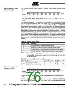
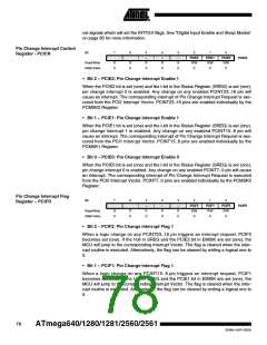
Pin Change Interrupt Control
Register - PCICR
Bit
7
6
5
–
4
–
3
–
2
PCIE2
R/W
0
1
PCIE1
R/W
0
0
PCIE0
R/W
0
PCICR
Read/Write
Initial Value
R
0
R
0
R
0
R
0
R
0
• Bit 2 – PCIE2: Pin Change Interrupt Enable 1
When the PCIE2 bit is set (one) and the I-bit in the Status Register (SREG) is set (one),
pin change interrupt 2 is enabled. Any change on any enabled PCINT23..16 pin will
cause an interrupt. The corresponding interrupt of Pin Change Interrupt Request is exe-
cuted from the PCI2 Interrupt Vector. PCINT23..16 pins are enabled individually by the
PCMSK2 Register.
• Bit 1 – PCIE1: Pin Change Interrupt Enable 1
When the PCIE1 bit is set (one) and the I-bit in the Status Register (SREG) is set (one),
pin change interrupt 1 is enabled. Any change on any enabled PCINT15..8 pin will
cause an interrupt. The corresponding interrupt of Pin Change Interrupt Request is exe-
cuted from the PCI1 Interrupt Vector. PCINT15..8 pins are enabled individually by the
PCMSK1 Register.
• Bit 0 – PCIE0: Pin Change Interrupt Enable 0
When the PCIE0 bit is set (one) and the I-bit in the Status Register (SREG) is set (one),
pin change interrupt 0 is enabled. Any change on any enabled PCINT7..0 pin will cause
an interrupt. The corresponding interrupt of Pin Change Interrupt Request is executed
from the PCI0 Interrupt Vector. PCINT7..0 pins are enabled individually by the PCMSK0
Register.
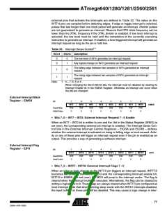
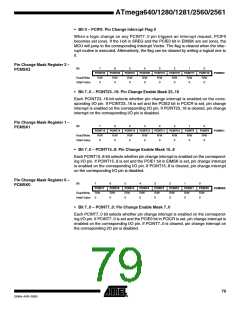
Pin Change Interrupt Flag
Register – PCIFR
Bit
7
6
5
–
4
–
3
–
2
PCIF2
R/W
0
1
PCIF1
R/W
0
0
PCIF0
R/W
0
PCIFR
Read/Write
Initial Value
R
0
R
0
R
0
R
0
R
0
• Bit 2 – PCIF2: Pin Change Interrupt Flag 1
When a logic change on any PCINT23..16 pin triggers an interrupt request, PCIF2
becomes set (one). If the I-bit in SREG and the PCIE2 bit in EIMSK are set (one), the
MCU will jump to the corresponding Interrupt Vector. The flag is cleared when the inter-
rupt routine is executed. Alternatively, the flag can be cleared by writing a logical one to
it.
• Bit 1 – PCIF1: Pin Change Interrupt Flag 1
When a logic change on any PCINT15..8 pin triggers an interrupt request, PCIF1
becomes set (one). If the I-bit in SREG and the PCIE1 bit in EIMSK are set (one), the
MCU will jump to the corresponding Interrupt Vector. The flag is cleared when the inter-
rupt routine is executed. Alternatively, the flag can be cleared by writing a logical one to
it.
78
ATmega640/1280/1281/2560/2561
2549A–AVR–03/05

 ATMEL [ ATMEL ]