ATmega640/1280/1281/2560/2561
external pins that activate the interrupts are defined in Table 33. The value on the
INT7:4 pins are sampled before detecting edges. If edge or toggle interrupt is selected,
pulses that last longer than one clock period will generate an interrupt. Shorter pulses
are not guaranteed to generate an interrupt. Observe that CPU clock frequency can be
lower than the XTAL frequency if the XTAL divider is enabled. If low level interrupt is
selected, the low level must be held until the completion of the currently executing
instruction to generate an interrupt. If enabled, a level triggered interrupt will generate an
interrupt request as long as the pin is held low.
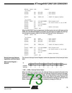
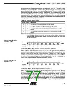
Table 33. Interrupt Sense Control(1)
ISCn1 ISCn0 Description
0
0
0
1
The low level of INTn generates an interrupt request.
Any logical change on INTn generates an interrupt request
The falling edge between two samples of INTn generates an interrupt
request.
1
0
The rising edge between two samples of INTn generates an interrupt
request.
1
1
Note:
1. n = 7, 6, 5 or 4.
When changing the ISCn1/ISCn0 bits, the interrupt must be disabled by clearing its
Interrupt Enable bit in the EIMSK Register. Otherwise an interrupt can occur when
the bits are changed.
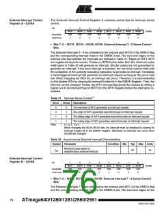
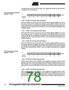
External Interrupt Mask
Register – EIMSK
Bit
7
6
5
4
3
2
1
0
IINT0
R/W
0
INT7
R/W
0
INT6
R/W
0
INT5
R/W
0
INT4
R/W
0
INT3
R/W
0
INT2
R/W
0
INT1
R/W
0
EIMSK
Read/Write
Initial Value
• Bits 7..0 – INT7 – INT0: External Interrupt Request 7 - 0 Enable
When an INT7 – INT0 bit is written to one and the I-bit in the Status Register (SREG) is
set (one), the corresponding external pin interrupt is enabled. The Interrupt Sense Con-
trol bits in the External Interrupt Control Registers – EICRA and EICRB – defines
whether the external interrupt is activated on rising or falling edge or level sensed. Activ-
ity on any of these pins will trigger an interrupt request even if the pin is enabled as an
output. This provides a way of generating a software interrupt.
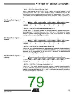
External Interrupt Flag
Register – EIFR
Bit
7
INTF7
R/W
0
6
INTF6
R/W
0
5
INTF5
R/W
0
4
INTF4
R/W
0
3
INTF3
R/W
0
2
INTF2
R/W
0
1
INTF1
R/W
0
0
IINTF0
R/W
0
EIFR
Read/Write
Initial Value
• Bits 7..0 – INTF7 - INTF0: External Interrupt Flags 7 - 0
When an edge or logic change on the INT7:0 pin triggers an interrupt request, INTF7:0
becomes set (one). If the I-bit in SREG and the corresponding interrupt enable bit,
INT7:0 in EIMSK, are set (one), the MCU will jump to the interrupt vector. The flag is
cleared when the interrupt routine is executed. Alternatively, the flag can be cleared by
writing a logical one to it. These flags are always cleared when INT7:0 are configured as
level interrupt. Note that when entering sleep mode with the INT3:0 interrupts disabled,
the input buffers on these pins will be disabled. This may cause a logic change in inter-
77
2549A–AVR–03/05

 ATMEL [ ATMEL ]